SGLS228C December 2003 – September 2015 TPS3805H33-Q1
PRODUCTION DATA.
- 1 Features
- 2 Applications
- 3 Description
- 4 Revision History
- 5 Device Comparison Table
- 6 Pin Configuration and Functions
- 7 Specifications
- 8 Detailed Description
- 9 Application and Implementation
- 10Power Supply Recommendations
- 11Layout
- 12Device and Documentation Support
- 13Mechanical, Packaging, and Orderable Information
9 Application and Implementation
NOTE
Information in the following applications sections is not part of the TI component specification, and TI does not warrant its accuracy or completeness. TI’s customers are responsible for determining suitability of components for their purposes. Customers should validate and test their design implementation to confirm system functionality.
9.1 Application Information
The TPS380x-Q1 voltage supervisor devices are designed to assert an active-low RESET signal when VDD and/or SENSE drop below a voltage threshold VIT. The RESET signal remains low until the voltages return above their respective thresholds. The TPS3803G15-Q1 and TPS3805H33-Q1 are fixed-voltage options, while the TPS3803-01-Q1 is adjustable and can be used to monitor any voltage above 1.226 V. The TPS3803G15-Q1 and TPS3803-01-Q1 have an open-drain output, requiring an external pull-up on the RESET line.
9.2 Typical Applications
9.2.1 TPS3803G15-Q1
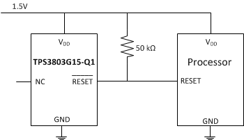 Figure 17. TPS3803G15 Typical Application
9.2.1.1 Design Requirements
When a single 1.5-V supply rail needs to be monitored, TPS3803G15-Q1 should be used. When a single voltage higher than 1.226 V needs to be monitored, TPS3803-01-Q1 should be used. When a 3.3-V supply and second supply above 1.226 V needs to be monitored, TPS3805H33-Q1 should be used.
9.2.1.2 Detailed Design Procedure
To monitor a single 1.5-V supply with TPS3803G15-Q1, connect the 1.5-V supply directly to VDD. The RESET output should be connected to the reset of the microcontroller with a pull-up resistor from the RESET output to VDD.
To monitor a single supply using TPS3803-01-Q1, connect the supply to VDD with a resistor divider to scale down the voltage at the SENSE pin. The resistor values must be chosen to satisfy Equation 1:
where
- VIT’ is the VDD threshold voltage.
For example, if TPS3803-01-Q1 should monitor a 2.5-V supply and the desired threshold voltage is 2.2 V, R1 and R2 values could be 24 kΩ and 30- kΩ respectively. A 1-nf to 10-nF decoupling capacitor is recommended to be placed close to the SENSE input.
To monitor two supplies using TPS3805H33-Q1, connect the 3.3-V supply directly to VDD, and the second supply through a resistor divider to the SENSE pin. The SENSE pin should have a 1-nf to 10-nF decoupling capacitor close to the pin.
9.2.1.3 Application Curves
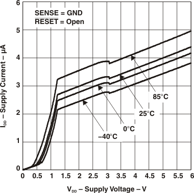
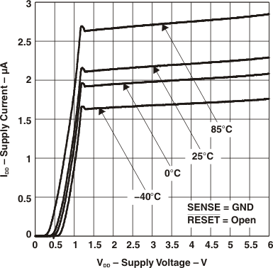
9.2.2 TPS3803-01-Q1
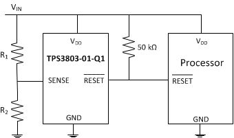 Figure 20. TPS3803-01-Q1 Typical Application
9.2.2.1 Design Requirements
Please refer to Design Requirements for this device's design requirements.
9.2.3 TPS3805H33-Q1
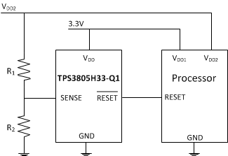 Figure 21. TPS3805H33-Q1 Typical Application
9.2.3.1 Design Requirements
Please refer to Design Requirements for this device's design requirements.