ZHCSF51A June 2016 – September 2016 TPS3779-Q1 , TPS3780-Q1
PRODUCTION DATA.
8 Detailed Description
8.1 Overview
The TPS3779-Q1 and TPS3780-Q1 are small, low quiescent current (IDD), dual-channel voltage detectors. These devices have high-accuracy rising and falling input thresholds, and assert the output as shown in Table 1. The output (OUTx pin) goes low when the SENSEx pin is less than VIT– and goes high when the pin is greater than VIT+. The TPS3779-Q1 and TPS3780-Q1 offer two hysteresis options (5% and 10%) for use in a wide variety of applications. These devices have two independent voltage-detection channels that can be used in systems where multiple voltage rails are required to be monitored, or where one channel can be used as an early warning signal and the other channel can be used as the system reset signal.
Table 1. TPS3779-Q1, TPS3780-Q1 Truth Table
| CONDITIONS | OUTPUT |
|---|---|
| SENSE1 < VIT– | OUT1 = low |
| SENSE2 < VIT– | OUT2 = low |
| SENSE1 > VIT+ | OUT1 = high |
| SENSE2 > VIT+ | OUT2 = high |
8.2 Functional Block Diagrams
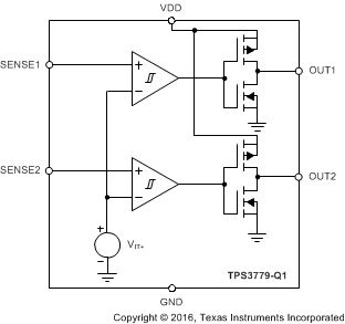
 Figure 20. TPS3779-Q1 Block Diagram
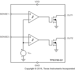
 Figure 21. TPS3780-Q1 Block Diagram
8.3 Feature Description
8.3.1 Inputs (SENSE1, SENSE2)
The TPS3779-Q1 and TPS3780-Q1 each have two comparators for voltage detection. Each comparator has one external input; the other input is connected to the internal reference. The comparator rising threshold is designed and trimmed to be equal to VIT+, and the falling threshold is trimmed to be equal to VIT–. The built-in falling hysteresis options make the devices immune to supply rail noise and ensure stable operation.
The comparator inputs can swing from ground to 5.5 V, regardless of the device supply voltage used. Although not required in most cases, for extremely noisy applications, good analog design practice is to place a 1-nF to 10-nF bypass capacitor at the comparator input in order to reduce sensitivity to transients and layout parasitic.
For each SENSEx input, the corresponding output (OUTx) is driven to logic low when the input voltage drops below VIT–. When the voltage exceeds VIT+, the output (OUTx) is driven high; see Figure 1.
8.3.2 Outputs (OUT1, OUT2)
In a typical device application, the outputs are connected to a reset or enable input of another device, such as a digital signal processor (DSP), central processing unit (CPU), field-programmable gate array (FPGA), or application-specific integrated circuit (ASIC); or the outputs are connected to the enable input of a voltage regulator, such as a dc-dc or low-dropout (LDO) regulator.
The TPS3779-Q1 provides two push-pull outputs. The logic high level of the outputs is determined by the VDD pin voltage. Pullup resistors are not required with this configuration, thus saving board space. However, all interface logic levels must be examined. All OUTx connections must be compatible with the VDD pin logic level.
The TPS3780-Q1 provides two open-drain outputs (OUT1 and OUT2); pullup resistors must be used to hold these lines high when the output goes to a high-impedance condition (not asserted). By connecting pullup resistors to the proper voltage rails, the outputs can be connected to other devices at correct interface voltage levels. The outputs can be pulled up to 5.5 V, independent of the device supply voltage. To ensure proper voltage levels, make sure to choose the correct pullup resistor values. The pullup resistor value is determined by VOL, the sink current capability, and the output leakage current (Ilkg(OD)). These values are specified in the Electrical Characteristics table. By using wired-AND logic, OUT1 and OUT2 can be combined into one logic signal. The Inputs (SENSE1, SENSE2) section describes how the outputs are asserted or deasserted. See Figure 1 for a description of the relationship between threshold voltages and the respective output.
8.4 Device Functional Modes
8.4.1 Normal Operation (VDD ≥ VDD(min))
When the voltage on VDD is greater than VDD(min) for tSD, the output signals react to the present state of the corresponding SENSEx pins.
8.4.2 Power-On-Reset (VDD < V(POR))
When the voltage on VDD is lower than the required voltage to internally pull the logic low output to GND (V(POR)), both outputs are undefined and are not to be relied upon for proper system function.