ZHCSUX4A July   2017  – February 2024 TPS3710-Q1

PRODUCTION DATA  

  1.   1
  2. 特性
  3. 应用
  4. 说明
  5. Pin Configuration and Functions
  6. Specifications
    1. 5.1 Absolute Maximum Ratings
    2. 5.2 ESD Ratings
    3. 5.3 Recommended Operating Conditions
    4. 5.4 Thermal Information
    5. 5.5 Electrical Characteristics
    6. 5.6 Timing Requirements
    7. 5.7 Switching Characteristics
    8. 5.8 Typical Characteristics
  7. Detailed Description
    1. 6.1 Overview
    2. 6.2 Functional Block Diagram
    3. 6.3 Feature Description
      1. 6.3.1 Input (SENSE)
      2. 6.3.2 Output (OUT)
      3. 6.3.3 Immunity to Input-Pin Voltage Transients
    4. 6.4 Device Functional Modes
      1. 6.4.1 Normal Operation (VDD > UVLO)
      2. 6.4.2 Undervoltage Lockout (V(POR) < VDD < UVLO)
      3. 6.4.3 Power-On Reset (VDD < V(POR))
  8. Application and Implementation
    1. 7.1 Application Information
      1. 7.1.1 VPULLUP to a Voltage Other Than VDD
      2. 7.1.2 Monitoring VDD
      3. 7.1.3 Monitoring a Voltage Other Than VDD
    2. 7.2 Typical Application
      1. 7.2.1 Design Requirements
      2. 7.2.2 Detailed Design Procedure
        1. 7.2.2.1 Resistor Divider Selection
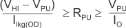
        2. 7.2.2.2 Pullup Resistor Selection
        3. 7.2.2.3 Input Supply Capacitor
        4. 7.2.2.4 Sense Capacitor
      3. 7.2.3 Application Curve
    3. 7.3 Do's and Don'ts
    4. 7.4 Power-Supply Recommendations
    5. 7.5 Layout
      1. 7.5.1 Layout Guidelines
      2. 7.5.2 Layout Example
  9. Device and Documentation Support
    1. 8.1 Device Support
      1. 8.1.1 Device Nomenclature
    2. 8.2 Documentation Support
      1. 8.2.1 Related Documentation
    3. 8.3 接收文档更新通知
    4. 8.4 支持资源
    5. 8.5 Trademarks
    6. 8.6 静电放电警告
    7. 8.7 术语表
  10. Revision History
  11. 10Mechanical, Packaging, and Orderable Information

封装选项

机械数据 (封装 | 引脚)
散热焊盘机械数据 (封装 | 引脚)
订购信息

Pullup Resistor Selection

To make ensure the proper voltage level, the pullup resistor value is selected by ensuring that the pullup voltage divided by the resistor does not exceed the sink-current capability of the device. This confirmation is calculated by verifying that the pullup voltage minus the output-leakage current (Ilkg(OD)) multiplied by the resistor is greater than the desired logic-high voltage. These values are specified in the Section 5.5.

Use Equation 2 to calculate the value of the pullup resistor.

Equation 2. GUID-D0AEBE83-7933-4567-8035-9699EAAA0321-low.gif