ZHCSHV0C June 2017 – April 2018 TPS2595
PRODUCTION DATA.
- 1 特性
- 2 应用
- 3 说明
- 4 修订历史记录
- 5 Device Comparison Table
- 6 Pin Configuration and Functions
- 7 Specifications
-
8 Detailed Description
- 8.1 Overview
- 8.2 Functional Block Diagram
- 8.3 Feature Description
- 8.4 Device Functional Modes
-
9 Application and Implementation
- 9.1 Application Information
- 9.2
Typical Application
- 9.2.1 Design Requirements
- 9.2.2 Detailed Design Procedure
- 9.2.3 Support Component Selection: CIN
- 9.2.4 Application Curves
- 9.2.5 Controlled Power Down (Quick Output Discharge) using TPS2595x5
- 9.2.6 Overvoltage Lockout using TPS259573
- 10Power Supply Recommendations
- 11Layout
- 12器件和文档支持
- 13机械、封装和可订购信息
7.7 Typical Characteristics
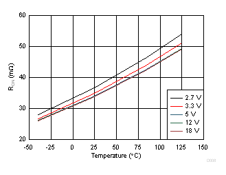
A.
Figure 3. On-resistance vs Temperature
| IOUT = 0.5A , Different Input Voltages |
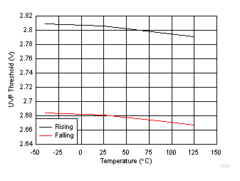
A.
Figure 5. UVP Threshold vs Temperature
| TPS2595x5 |
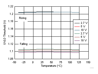
A.
Figure 7. UVLO Threshold vs Temperature
| TPS2595x0/1/5, Different Input Voltages |
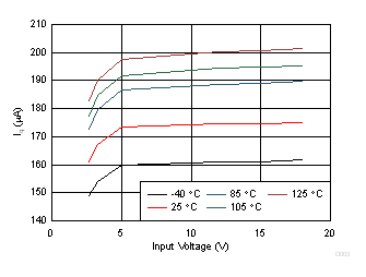
A.
Figure 9. Quiescent Current vs Input Voltage
A.
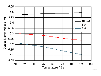
Figure 11. OVC Threshold vs Temperature
| TPS25953x, Different Output Load Currents |
A.
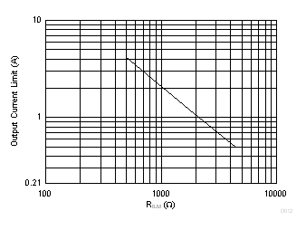
Figure 13. Output Current Limit (ILIMIT) vs RILM
A.
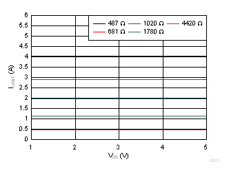
Figure 15. Output Current Limit vs VDS
| Different RILM values |
A.
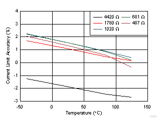
Figure 17. Output Current Limit Accuracy vs Temperature
| VIN = 3.3 V, Different RILM values |
A.
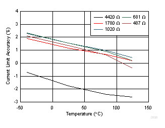
Figure 19. Output Current Limit Accuracy vs Temperature
| VIN = 12 V, Different RILM values |
A.
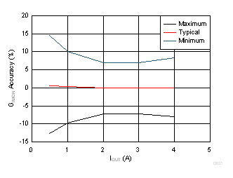
Figure 21. Load Current Monitor Gain Accuracy vs Load Current
| Normalized to reference value of GIMON = 276uA/A |
A.
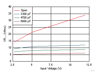
Figure 23. ON Slew Rate vs Input Voltage
| Different CdVdt values |
A.
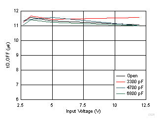
Figure 25. Turn OFF Delay vs Input Voltage
| Different CdVdt values |
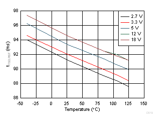
A.
Figure 27. Thermal Shutdown Auto-Retry Interval vs Temperature
| TPS2595x1/3/5, Different Input Voltages |
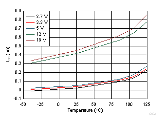
A.
Figure 4. Shutdown Current vs Temperature
| TPS2595x0/1/5, EN=GND, OUT=Open, Different Input Voltages |
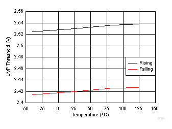
A.
Figure 6. UVP Threshold vs Temperature
| TPS2595x0/1/3 |
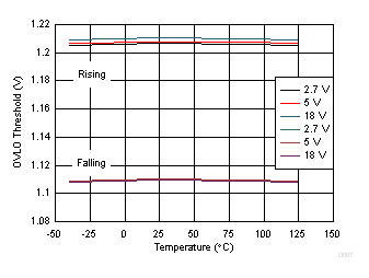
A.
Figure 8. OVLO Threshold vs Temperature
| TPS259573, Different Input Voltages |
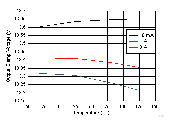
A.
Figure 10. OVC Threshold vs Temperature
| TPS25954x, Different Output Load Currents |
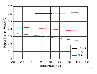
A.
Figure 12. OVC Threshold vs Temperature
| TPS25952x, Different Output Load Currents |
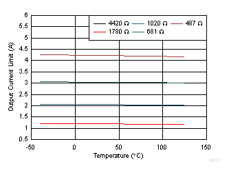
A.
Figure 14. Output Current Limit (ILIMIT) vs Temperature
| VIN = 12V, Different RILM values |
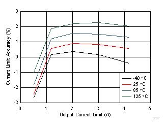
A.
Figure 16. Output Current Limit Accuracy vs Output Current Limit
| VIN = 5 V |
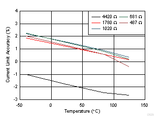
A.
Figure 18. Output Current Limit Accuracy vs Temperature
| VIN = 5 V, Different RILM values |
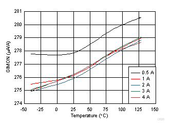
A.
Figure 20. Load Current Monitor Gain vs Temperature
| Different Output Load Currents |
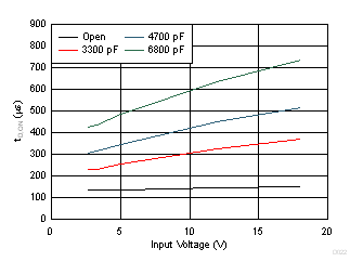
A.
Figure 22. Turn on Delay vs Input Voltage
| Different CdVdt values |
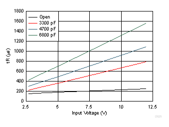
A.
Figure 24. Rise Time vs Input Voltage
| Different CdVdt values |
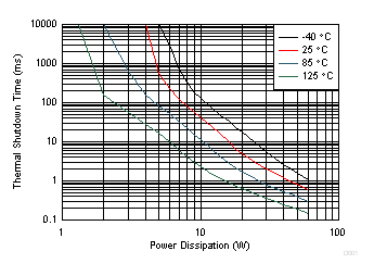
A.
Figure 26. Thermal Shutdown Time vs Power Dissipation
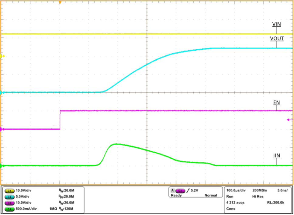
| VIN = 12 V, COUT = 10 µF, RILM = 487 Ω, VEN = 5 V |
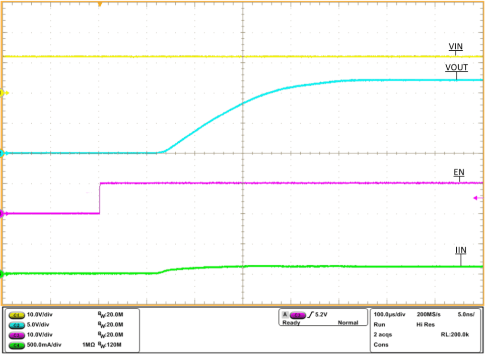
1.
Figure 30. Turn ON Delay
| VIN = 12 V, COUT = 1 µF, RILM = 487 Ω, ROUT = 100 Ω |
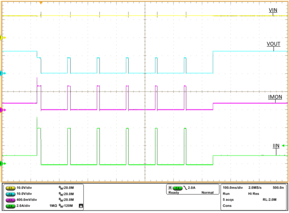
1.
Figure 32. TPS2595x1, TPS2595x3, TPS2595x5 OverCurrent Response
| VIN = 12 V, COUT = 1 µF, RILM = 487 Ω, ROUT varied from 12 Ω to 2 Ω to 12 Ω |
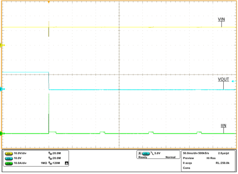
1.
Figure 34. Output Hot Short to GND Response
| VIN = 12 V, COUT = 1 µF, RILM = 487 Ω |
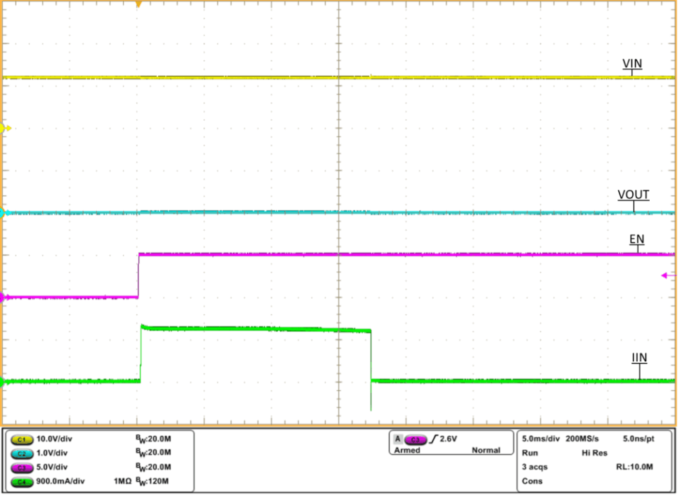
1.
Figure 36. Wake Up With Output Short to GND
| VIN = 12 V, COUT = 1 µF, RILM = 487 Ω |
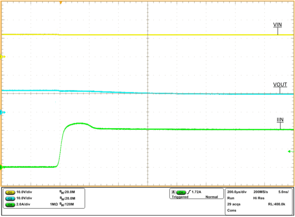
1.
Figure 38. Output Load Transient Response
| VIN = 12 V, COUT = 1 µF, RILM = 487 Ω, IOUT stepped from 4 A to 4.8 A |
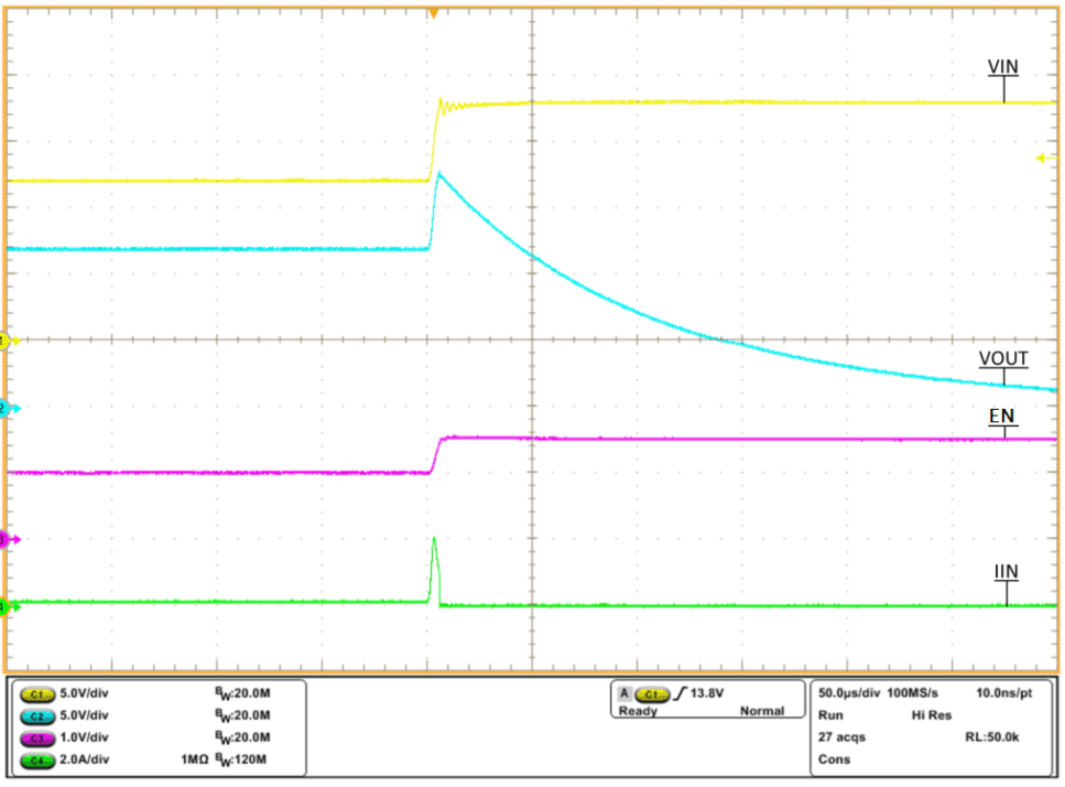
1.
Figure 40. TPS259573 Overvoltage Lockout Response
| VIN stepped from 12 V to 18 V, COUT = 1 µF, RILM = 487 Ω, FLT = 3.3 V through 10 kΩ, ROUT = 100 Ω |
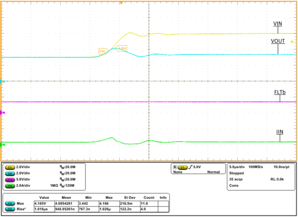
1.
Figure 42. TPS25952x Overvoltage Clamp Response
| VIN stepped from 3 V to 6 V, COUT = 1 µF, RILM = 487 Ω, FLT= 3.3 V through 10 kΩ, ROUT = 10 Ω |
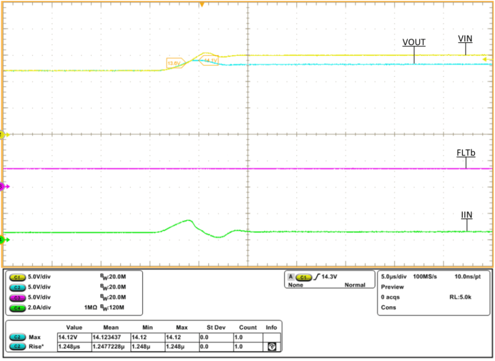
1.
Figure 44. TPS25954x Overvoltage Clamp Response
| VIN Stepped from 12 V to 15 V, COUT = 1 µF, RILM = 487 Ω, FLT = 3.3 V through 10 kΩ, ROUT = 20 Ω |
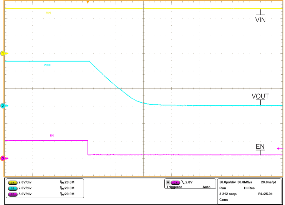
1.
Figure 46. TPS2595x5 Quick Output Discharge, EN stepped from 5 V to 1 V
| VIN = 5 V, COUT = 1 µF, RILM = 487 Ω |
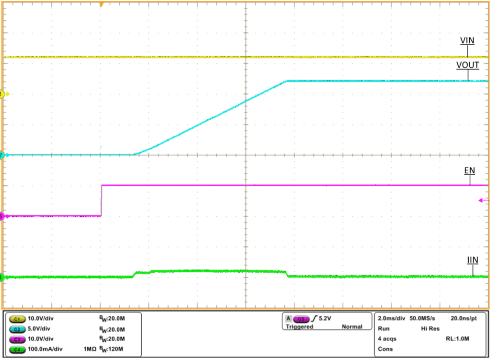
1.
Figure 29. Output Voltage Ramp and Inrush Current at Start Up, CdVdT = 22 nF
| VIN = 12 V, COUT = 10 µF, RILM = 487 Ω, VEN = 5 V |
1.
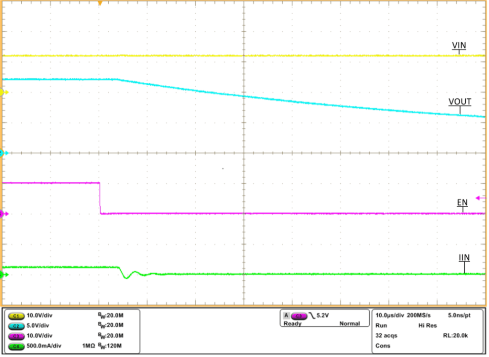
Figure 31. Turn OFF Delay
| VIN = 12 V, COUT = 1 µF, RILM = 487 Ω, ROUT = 100 Ω |
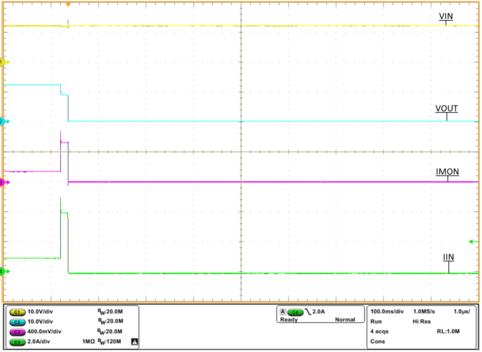
1.
Figure 33. TPS2595x0 Overcurrent Response
| VIN = 12 V, COUT = 1 µF, RILM = 487 Ω, ROUT varied from 12 Ω to 2 Ω to 12 Ω |
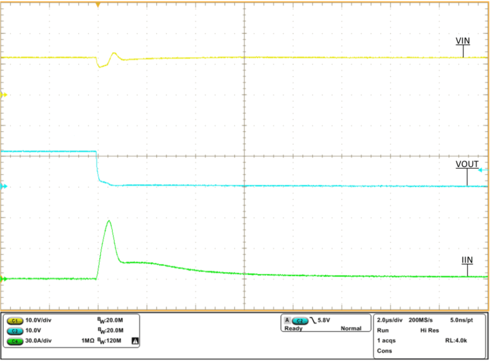
1.
Figure 35. Output Hot Short to GND Response (Zoomed In)
| VIN = 12 V, COUT = 1 µF, RILM = 487 Ω |
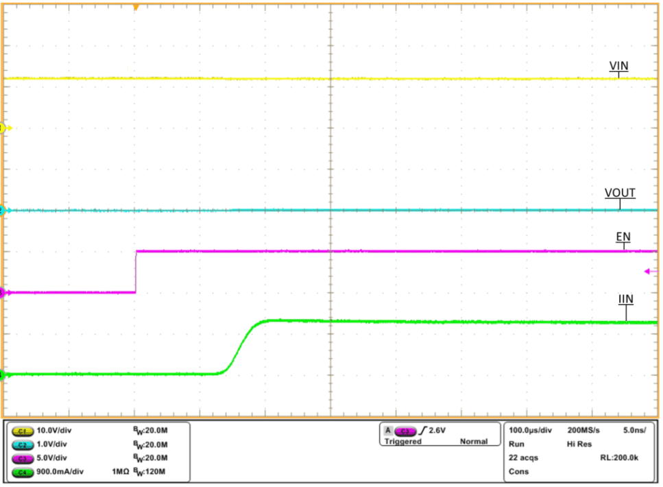
1.
Figure 37. Wake Up With Output Short to GND (Zoomed In)
| VIN = 12 V, COUT = 1 µF, RILM = 487 Ω |
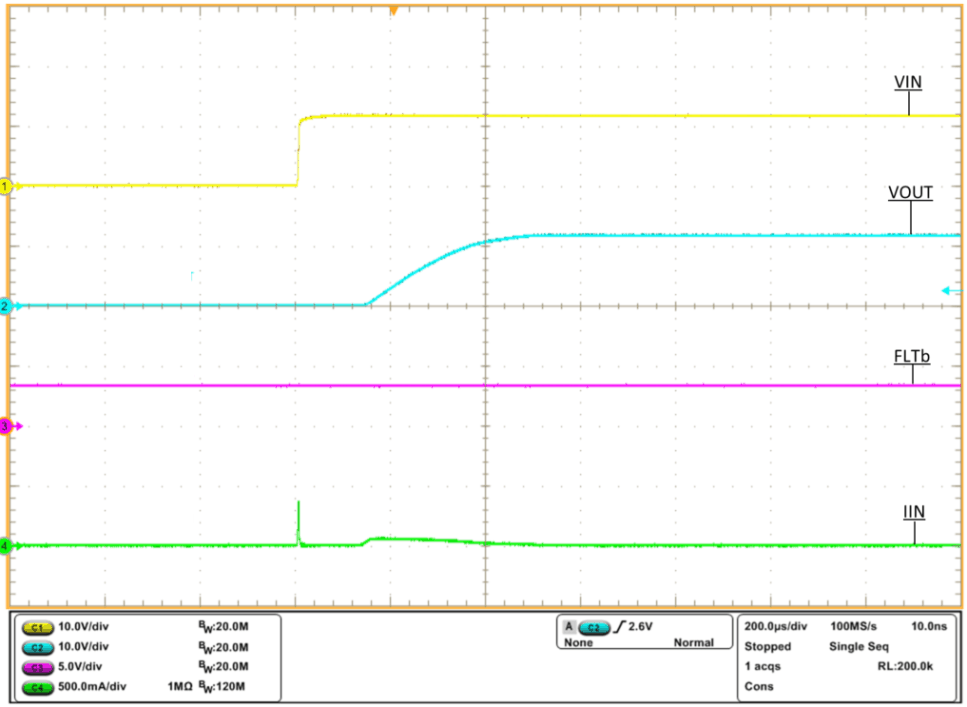
1.
Figure 39. Hot Plug Response
| VIN = 12 V, COUT = 1 µF, RILM = 487 Ω, FLT = 3.3 V through 10 kΩ |
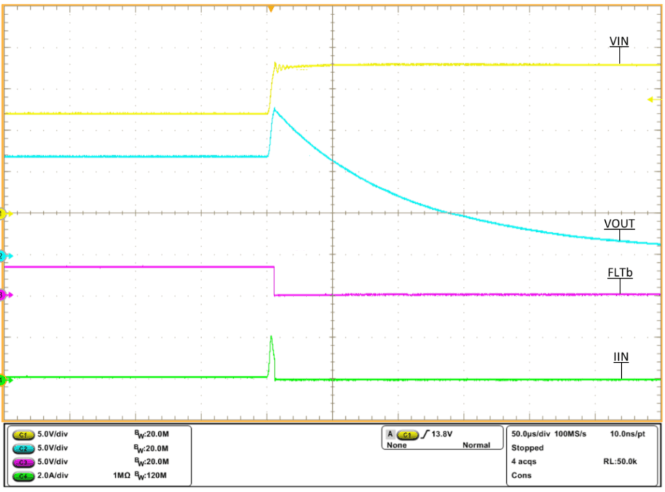
1.
Figure 41. TPS259573 Overvoltage Lockout FLT Response
| VIN stepped from 12 V to 18 V, COUT = 1 µF, RILM = 487 Ω, FLT = 3.3 V through 10 kΩ, ROUT = 100 Ω |
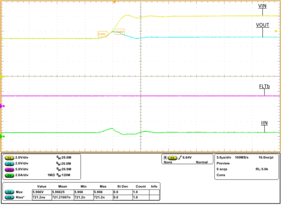
1.
Figure 43. TPS25953x Overvoltage Clamp Response
| VIN stepped from 5 V to 8 V, COUT = 1 µF, RILM = 487 Ω, FLT = 3.3 V through 10 kΩ, ROUT = 10 Ω |
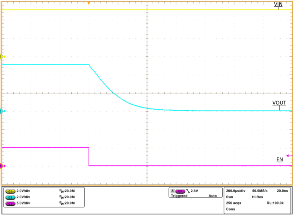
1.
Figure 45. TPS2595x5 Quick Output Discharge, EN stepped from 5 V to 0 V
| VIN = 5 V, COUT = 1 µF, RILM = 487 Ω |