ZHCSCK2 June 2014
PRODUCTION DATA.
- 1 特性
- 2 应用范围
- 3 说明
- 4 简化电路原理图
- 5 修订历史记录
- 6 Pin Configuration and Functions
- 7 Specifications
- 8 Parametric Measurement Information
-
9 Detailed Description
- 9.1 Overview
- 9.2 Functional Block Diagram
- 9.3
Feature Description
- 9.3.1 Enable and Adjusting Undervoltage Lockout
- 9.3.2 Overvoltage Protection (OVP)
- 9.3.3 Hot Plug-in and In-Rush Current Control
- 9.3.4 Overload and Short Circuit Protection :
- 9.3.5 FAULT Response
- 9.3.6 Current Monitoring:
- 9.3.7 Power Good Comparator
- 9.3.8 IN, OUT and GND Pins
- 9.3.9 Thermal Shutdown:
- 9.4 Device Functional Modes
-
10Application and Implementation
- 10.1 Application Information
- 10.2
Typical Application
- 10.2.1
eFuse for Enterprise SSDs
- 10.2.1.1 Design Requirements
- 10.2.1.2
Detailed Design Procedure
- 10.2.1.2.1 Step by Step Design Procedure
- 10.2.1.2.2 Programming the Current-Limit Threshold: R(ILIM) Selection
- 10.2.1.2.3 Undervoltage Lockout and Overvoltage Set Point
- 10.2.1.2.4 Programming Current Monitoring Resistor - RIMON
- 10.2.1.2.5 Setting Output Voltage Ramp time (tdVdT)
- 10.2.1.2.6 Programing the Power Good Set Point
- 10.2.1.2.7 Support Component Selections - R6, R7 and CIN
- 10.2.1.3 Application Curves
- 10.2.1
eFuse for Enterprise SSDs
- 10.3 System Examples
- 11Power Supply Recommendations
- 12Layout
- 13器件和文档支持
- 14机械封装和可订购信息
6 Pin Configuration and Functions
TPS25940
RVC PACKAGE
(TOP VIEW)
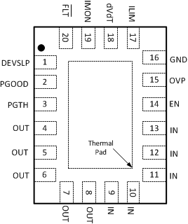
Pin Functions
| NAME | NO. | I/O | DESCRIPTION |
|---|---|---|---|
| DEVSLP | 1 | I | Active High. DevSleep Mode control. A high at this pin will activate the DevSleep mode(Low Power Mode). |
| PGOOD | 2 | O | Active High. A high indicates PGTH has crossed the threshold value. It is an open drain output. |
| PGTH | 3 | I | Positive input of PGOOD comparator. |
| OUT | 4 - 8 | O | Power Output of the device. |
| IN | 9 - 13 | I | Power Input and supply voltage of the device. |
| EN/UVLO | 14 | I | Input for setting programmable undervoltage lockout threshold. An undervoltage event will open internal FET and assert FLT to indicate power-failure. When pulled to GND, resets the fault latch in TPS25940L. |
| OVP | 15 | I | Input for setting programmable overvoltage protection threshold. An overvoltage event will open the internal FET and assert FLT to indicate overvoltage. |
| GND | 16 | — | Ground. |
| ILIM | 17 | I/O | A resistor from this pin to GND sets the overload and short-circuit current limit. |
| dVdT | 18 | I/O | A capacitor from this pin to GND sets the ramp rate of output voltage. |
| IMON | 19 | O | This pin sources a scaled down ratio of current through the internal FET. A resistor from this pin to GND converts current to proportional voltage, used as analog current monitor. |
| FLT | 20 | O | Fault event indicator, goes low to indicate fault condition due to Undervoltage, Overvoltage, Reverse voltage and Thermal shutdown event. It is an open drain output. |
| PowerPADTM | The GND terminal must be connected to the exposed PowerPAD. This PowerPAD must be connected to a PCB ground plane using multiple vias for good thermal performance. | ||