ZHCSF29E May 2016 – January 2021 TPS25940-Q1
PRODMIX
- 1 特性
- 2 应用
- 3 说明
- 4 Revision History
- 5 Device Comparison Table
- 6 Pin Configuration and Functions
- 7 Specifications
- 8 Parametric Measurement Information
-
9 Detailed Description
- 9.1 Overview
- 9.2 Functional Block Diagram
- 9.3 Feature Description
- 9.4 Device Functional Modes
-
10Application and Implementation
- 10.1 Application Information
- 10.2
Typical Application
- 10.2.1 Design Requirements
- 10.2.2
Detailed Design Procedure
- 10.2.2.1 Step by Step Design Procedure
- 10.2.2.2 Programming the Current-Limit Threshold: R(ILIM) Selection
- 10.2.2.3 Undervoltage Lockout and Overvoltage Set Point
- 10.2.2.4 Programming Current Monitoring Resistor—RIMON
- 10.2.2.5 Setting Output Voltage Ramp Time (tdVdT)
- 10.2.2.6 Programing the Power Good Set Point
- 10.2.2.7 Support Component Selections—R6, R7 and CIN
- 10.2.3 Application Curves
- 10.2.4 System Examples
- 11Power Supply Recommendations
- 12Layout
- 13Device and Documentation Support
- 14Mechanical, Packaging, and Orderable Information
7.7 Typical Characteristics
Conditions are –40°C ≤ TA = TJ ≤ 125°C, V(IN) = 12 V, V(EN/UVLO) = 2 V, V(OVP) = V(DEVSLP) = V(PGTH) = 0 V, R(ILIM) = 150 kΩ, C(OUT) = 1 µF, C(dVdT) = OPEN, PGOOD =
FLT = IMON = OPEN. (unless stated otherwise)
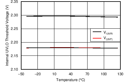 Figure 7-1 UVLO Threshold Voltage vs Temperature
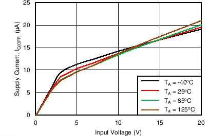 Figure 7-3 Input Supply Current vs Supply Voltage at Shutdown
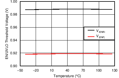 Figure 7-5 EN Threshold Voltage vs Temperature
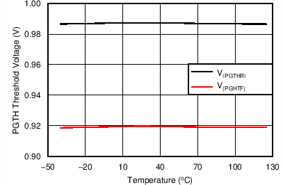 Figure 7-7 PGTH Threshold Voltage vs Temperature
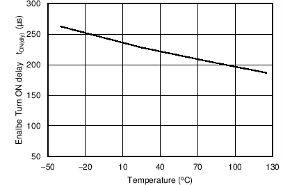 Figure 7-9 Enable Turn ON Delay vs Temperature
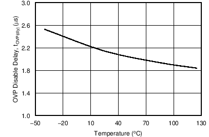 Figure 7-11 OVP Disable Delay vs Temperature
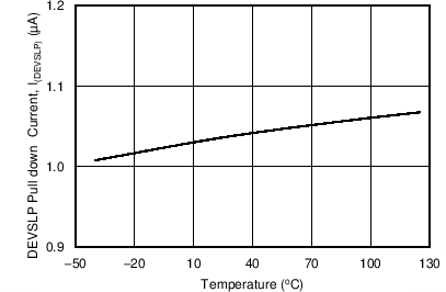 Figure 7-13 DEVSLP Pull Down Current vs Temperature
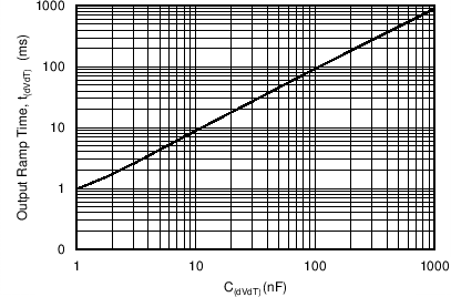 Figure 7-15 Output Ramp Time vs C(dVdT)
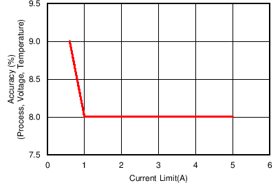 Figure 7-17 Current Limit Accuracy vs Current Limit
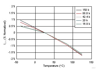 Figure 7-19 Current Limit (% Normalized) vs R(LIMIT) Resistor
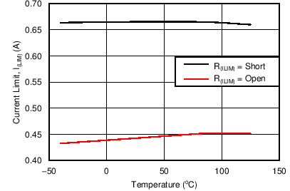 Figure 7-21 Current Limit for R(ILIM) = Open and Short vs Temperature
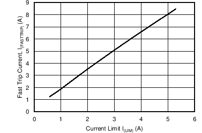 Figure 7-23 Fast Trip Threshold vs Current Limit
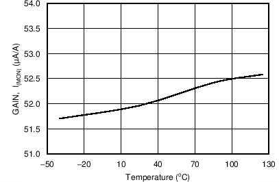 Figure 7-25 GAIN(IMON) vs Temperature
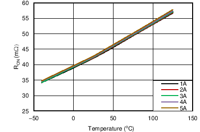 Figure 7-27 RON vs Temperature Across Load Current
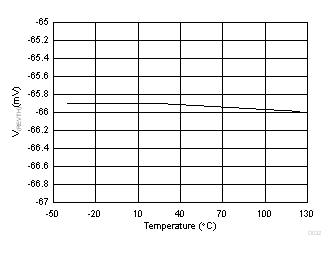 Figure 7-29 V(REVTH) vs Temperature
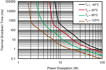
| Taken on 2-Layer board, 2 oz.(0.08-mm thick) with GND plane area: 14 cm2 (Top) and 20 cm2 (bottom) |
| V(IN) = 11 V |
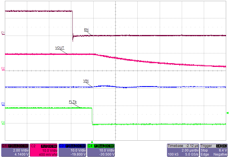
| R( FLT)=100 kΩ |
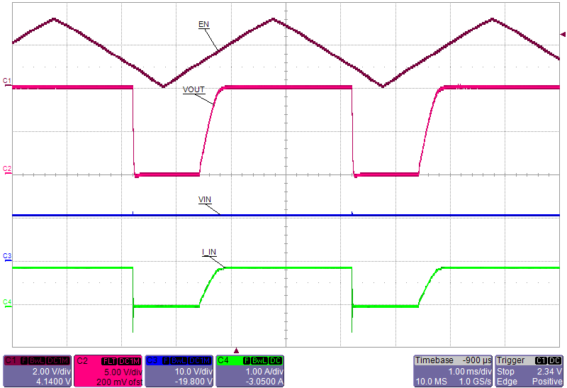
| V(IN) = 12 V | RL = 12 Ω | R( FLT)=100 kΩ |
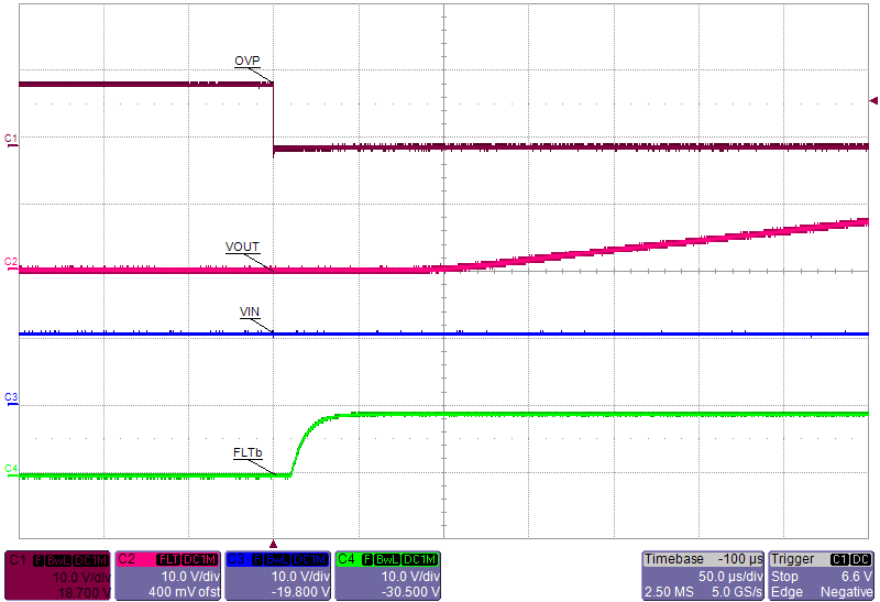
| V(IN) = 12 V | RL = 12 Ω | R( FLT)= 100 kΩ |
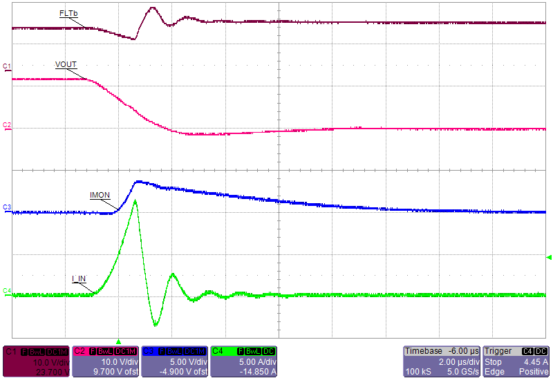
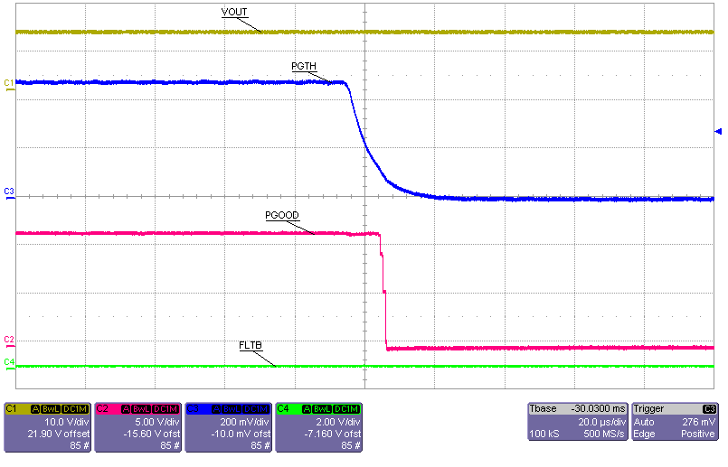
| R( FLT)= 100 kΩ | R(IMON) = 16.9 kΩ | R(ILIM) = 17.8 kΩ |
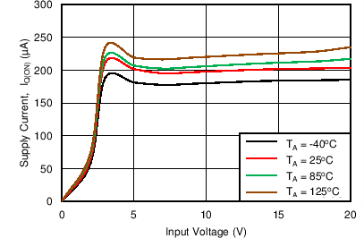 Figure 7-2 Input Supply Current vs
Supply Voltage During Normal Operation
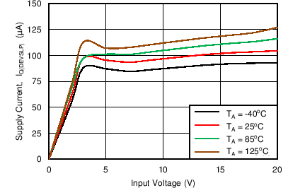 Figure 7-4 Input Supply Current vs Supply Voltage in DevSleep Mode
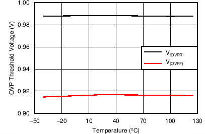 Figure 7-6 OVP Threshold Voltage vs Temperature
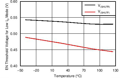 Figure 7-8 EN Threshold Voltage for Low IQ Mode vs Temperature
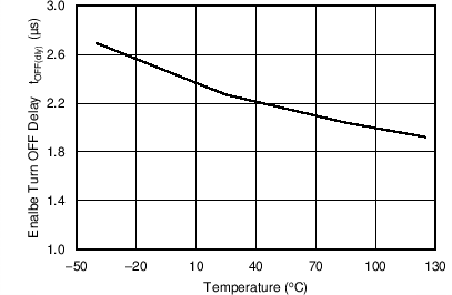 Figure 7-10 Enable Turn OFF Delay vs Temperature
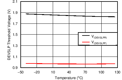 Figure 7-12 DEVSLP Threshold Voltage vs Temperature
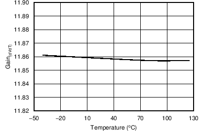 Figure 7-14 GAIN(dVdT) vs Temperature
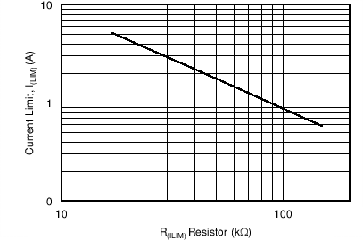 Figure 7-16 Current Limit vs Current Limit Resistor
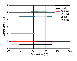 Figure 7-18 Current Limit vs Temperature Across R(ILIM)
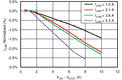
| Thermal shutdown occurs when I(LIM) = 5.3 A | [V(IN) - V(OUT)] > 8 V | |
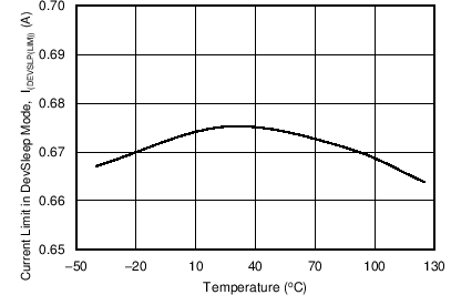 Figure 7-22 Current Limit in DevSleep Mode vs Temperature
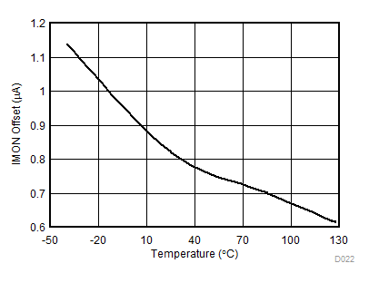 Figure 7-24 IMON Offset vs Temperature
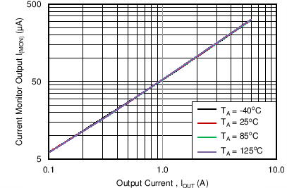 Figure 7-26 Current Monitor Output vs Output Current
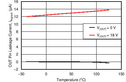 Figure 7-28 OUT Leakage Current in Off State vs Temperature
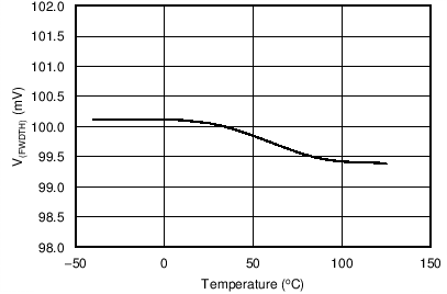 Figure 7-30 V(FWDTH) vs Temperature
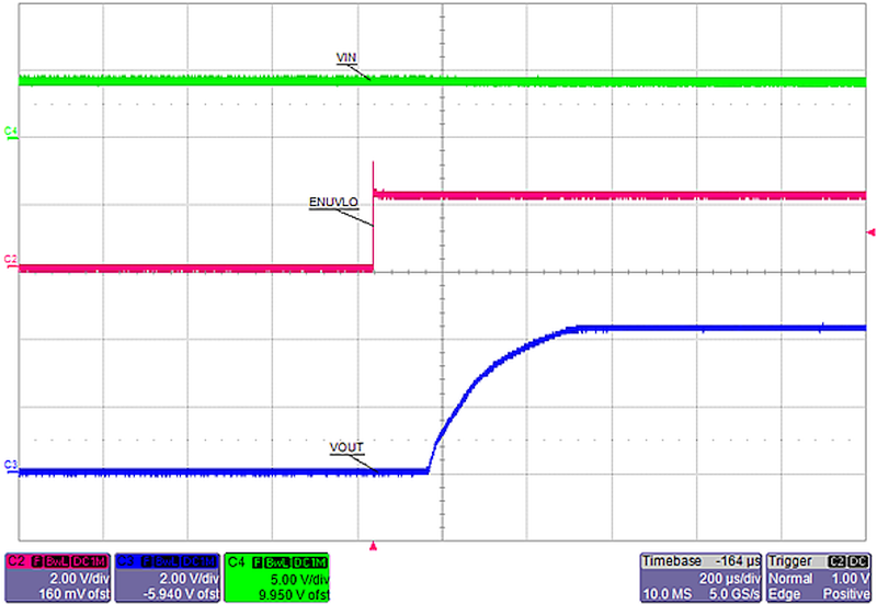
| V(IN) = 4.5 V |
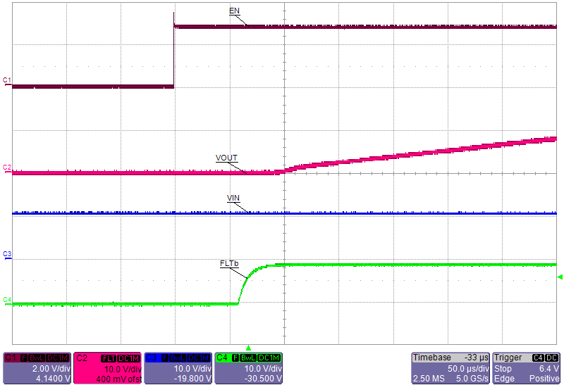
| R( FLT)=100 kΩ |
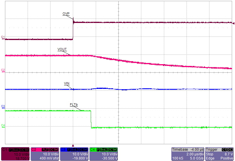
| V(IN) = 12 V | RL = 12 Ω | R( FLT)=100 kΩ |
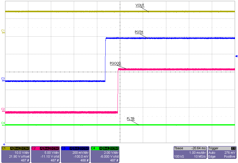
| V(IN) = 12 V | RL = 12 Ω | R( FLT)= 100 kΩ |
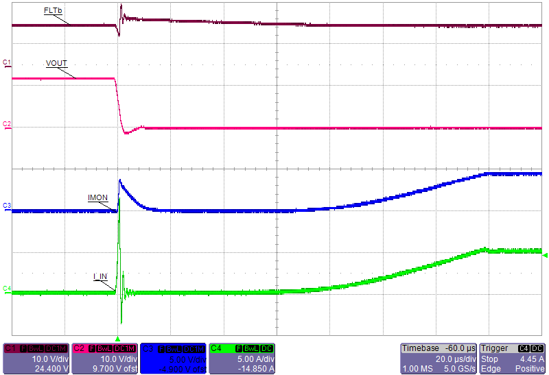
| R( FLT) = 100 kΩ | R(IMON) = 16.9 kΩ | R(ILIM) = 17.8 kΩ |