ZHCSLL2A May 2021 – March 2022 TPS25830A-Q1 , TPS25832A-Q1
PRODUCTION DATA
- 1 特性
- 2 应用
- 3 说明
- 4 Revision History
- 5 说明(续)
- 6 Device Comparison Table
- 7 Pin Configuration and Functions
- 8 Specifications
- 9 Parameter Measurement Information
-
10Detailed Description
- 10.1 Overview
- 10.2 Functional Block Diagram
- 10.3
Feature Description
- 10.3.1 Buck Regulator
- 10.3.2 Enable/UVLO and Start-Up
- 10.3.3 Switching Frequency and Synchronization (RT/SYNC)
- 10.3.4 Spread-Spectrum Operation
- 10.3.5 VCC, VCC_UVLO
- 10.3.6 Minimum ON-Time, Minimum OFF-Time
- 10.3.7 Internal Compensation
- 10.3.8 Bootstrap Voltage (BOOT)
- 10.3.9 RSNS, RSET, RILIMIT and RIMON
- 10.3.10 Overcurrent and Short Circuit Protection
- 10.3.11 Overvoltage, IEC and Short to Battery Protection
- 10.3.12 Cable Compensation
- 10.3.13 USB Port Control
- 10.3.14 FAULT Response
- 10.3.15 USB Specification Overview
- 10.3.16 USB Type-C® Basics
- 10.3.17 Device Power Pins (IN, CSN/OUT, and PGND)
- 10.3.18 Thermal Shutdown
- 10.3.19 Power Wake
- 10.4 Device Functional Modes
-
11Application and Implementation
- 11.1 Application Information
- 11.2
Typical Application
- 11.2.1 Design Requirements
- 11.2.2
Detailed Design Procedure
- 11.2.2.1 Output Voltage
- 11.2.2.2 Switching Frequency
- 11.2.2.3 Inductor Selection
- 11.2.2.4 Output Capacitor Selection
- 11.2.2.5 Input Capacitor Selection
- 11.2.2.6 Bootstrap Capacitor Selection
- 11.2.2.7 VCC Capacitor Selection
- 11.2.2.8 Enable and Undervoltage Lockout Set-Point
- 11.2.2.9 Current Limit Set-Point
- 11.2.2.10 Cable Compensation Set-Point
- 11.2.2.11 LD_DET, POL, and FAULT Resistor Selection
- 11.2.3 Application Curves
- 12Power Supply Recommendations
- 13Layout
- 14Device and Documentation Support
- 15Mechanical, Packaging, and Orderable Information
10.3.10.2 Current Limit Setting for MFI OCP
Apple has defined new overcurrent protection requirements in its latest MFI spec. TPS2583xA-Q1 also implements a novel current limit inside to meet the MFI OC requirement.
The settings are described below:
- With external MOSFET: When
TPS2583xA-Q1 uses an external FET for current limit, it actually has two
current limit threshold. The 1st threshold ILIMIT1 is determined
by RLIMIT according to equation 6. The 2nd threshold
ILIMIT2 equals to 1.6 times of ILIMIT1.
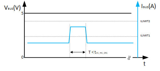
- Case 1: If the load
current IBUS is in the range ILIMIT2 >
IBUS > ILIMIT1, and the duration <
tOC_HIC_DEG, the external MOSFET will remain on and
VBUS will stay unchanged, as shown in #FIG_CXG_5M1_LPB.
 Figure 10-18 Two level Current Limit
Methodology with ext MOSFET Case 1
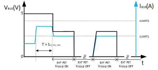
 - Case 2: If the load
current IBUS is in the range ILIMIT2 >
IBUS > ILIMIT1 and the duration >
tOC_HIC_DEG, the external MOSFET will current limit
to ILIMIT1, then enter hiccup mode with 2 ms of on-time
and 263 ms of off-time, as shown in #GUID-16FE87EA-B025-4988-A10B-2C1D9B306751. When the load current decreases below ILIMIT1 and
continues > tOC_HIC_RST, the external MOSFET will
resume always on.
 Figure 10-19 Two Level
Current Limit Methodology with ext MOSFET Case 2
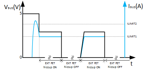
 - Case 3: If the load
current IBUS > ILIMIT2, the external MOSFET
will current limit to ILIMIT1 immediately, then enter
hiccup mode with 2 ms of on-time and 263 ms of off-time, as shown in
#GUID-528C297C-06CA-420F-93DB-04BF78DC50B0. When the load current IBUS < ILIMIT1
for tOC_HIC_RST, the external MOSFET will resume always
on.
 Figure 10-20 Two Level
Current Limit Methodology with ext MOSFET Case 3
- Case 1: If the load
current IBUS is in the range ILIMIT2 >
IBUS > ILIMIT1, and the duration <
tOC_HIC_DEG, the external MOSFET will remain on and
VBUS will stay unchanged, as shown in #FIG_CXG_5M1_LPB.
- Buck average current limit
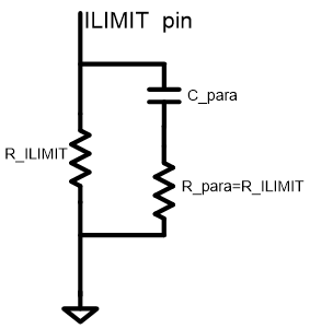
- When TPS2583xA-Q1 uses Buck average current limit, it has only one current limit threshold determined by RLIMIT according to GUID-A4E3DF06-CF74-42E0-870E-829A84694818.html#EQUATION-BLOCK_OMH_F53_NPB.
- In order to meet the MFI OC requirement, an RC network is needed in parallel with Rlimit resistor as shown in #FIG_YB3_1TQ_1NB. Suggest selecting Rpara = Rlimit, Cpara = 100 nF.
 Figure 10-21 RC Network in
Parallel with Rlimit