ZHCSC59A March 2014 – June 2014 TPS2561A-Q1
PRODUCTION DATA.
- 1 特性
- 2 应用范围
- 3 说明
- 4 修订历史记录
- 5 Device Comparison Table
- 6 Pin Functions and Configurations
- 7 Specifications
- 8 Parameter Measurement Information
- 9 Detailed Description
-
10Application and Implementation
- 10.1 Application Information
- 10.2
Typical Application
- 10.2.1
Design Current Limit
- 10.2.1.1 Design Requirements
- 10.2.1.2
Detailed Design Procedure
- 10.2.1.2.1 Determine Design Parameters
- 10.2.1.2.2 Programming the Current-Limit Threshold
- 10.2.1.2.3 Designing Above a Minimum Current Limit
- 10.2.1.2.4 Designing Below a Maximum Current Limit
- 10.2.1.2.5 Accounting for Resistor Tolerance
- 10.2.1.2.6 Power Dissipation and Junction Temperature
- 10.2.1.2.7 Auto-Retry Functionality
- 10.2.1.2.8 Two-Level Current-Limit Circuit
- 10.2.2 Application Curves
- 10.2.1
Design Current Limit
- 11Power Supply Requirements
- 12Layout
- 13器件和文档支持
- 14机械封装和可订购信息
9 Detailed Description
9.1 Overview
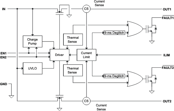
The TPS2561A-Q1 is a dual-channel, current-limited power-distribution switch using N-channel MOSFETs for automotive applications where short circuits or heavy capacitive loads will be encountered. This device allows the user to program the current-limit threshold between 250 mA and 2.8 A (typ) per channel via an external resistor. This device incorporates an internal charge pump and gate drive circuitry necessary to drive the N-channel MOSFETs. The charge pump supplies power to the driver circuit for each channel and provides the necessary voltage to pull the gate of the MOSFET above the source. The charge pump operates from input voltages as low as 2.5 V and requires little supply current. The driver controls the gate voltage of the power switch. The driver incorporates circuitry that controls the rise and fall times of the output voltage to limit large current and voltage surges and provides built-in soft-start functionality. Each channel of the TPS2561A-Q1 limits the output current to the programmed current-limit threshold IOS during an overcurrent or short-circuit event by reducing the charge pump voltage driving the N-channel MOSFET and operating it in the linear range of operation. The result of limiting the output current to IOS reduces the output voltage at OUTx because the N-channel MOSFET is no longer fully enhanced.
9.2 Functional Block Diagram
9.3 Feature Description
9.3.1 Overcurrent Conditions
The TPS2561A-Q1 responds to overcurrent conditions by limiting the output current per channel to IOS. When an overcurrent condition is detected, the device maintains a constant output current and reduces the output voltage accordingly. Two possible overload conditions can occur.
The first condition is when a short circuit or partial short circuit is present when the device is powered-up or enabled. The output voltage is held near zero potential with respect to ground and the TPS2561A-Q1 ramps the output current to IOS. The TPS2561A-Q1 devices will limit the current to IOS until the overload condition is removed or the device begins to thermal cycle.
The second condition is when a short circuit, partial short circuit, or transient overload occurs while the device is enabled and powered on. The device responds to the overcurrent condition within time tIOS (see Figure 10). The current-sense amplifier is overdriven during this time and momentarily disables the internal current-limit MOSFET. The current-sense amplifier recovers and ramps the output current to IOS. Similar to the previous case, the TPS2561A-Q1 will limit the current to IOS until the overload condition is removed or the device begins to thermal cycle.
The TPS2561A-Q1 thermal cycles if an overload condition is present long enough to activate thermal limiting in any of the above cases. The device turns off when the junction temperature exceeds 135°C (min) while in current limit. The device remains off until the junction temperature cools 20°C (typ) and then restarts. The TPS2561A-Q1 cycles on/off until the overload is removed (see Figure 20) .
9.3.2 FAULTx Response
The FAULTx open-drain outputs are asserted (active low) on an individual channel during an overcurrent or overtemperature condition. The TPS2561A-Q1 asserts the FAULTx signal until the fault condition is removed and the device resumes normal operation on that channel. The TPS2561A-Q1 is designed to eliminate false FAULTx reporting by using an internal delay "deglitch" circuit (9-ms typ) for overcurrent conditions without the need for external circuitry. This ensures that FAULTx is not accidentally asserted due to normal operation such as starting into a heavy capacitive load. The deglitch circuitry delays entering and leaving current-limited induced fault conditions. The FAULTx signal is not deglitched when the MOSFET is disabled due to an overtemperature condition but is deglitched after the device has cooled and begins to turn on. This unidrectional deglitch prevents FAULTx oscillation during an overtemperature event.
9.3.3 Thermal Sense
The TPS2561A-Q1 self protects by using two independent thermal sensing circuits that monitor the operating temperature of the power switch and disable operation if the temperature exceeds recommended operating conditions. Each channel of the TPS2561A-Q1 operates in constant-current mode during an overcurrent conditions, which increases the voltage drop across the power switch. The power dissipation in the package is proportional to the voltage drop across the power switch, which increases the junction temperature during an overcurrent condition. The first thermal sensor (OTSD) turns off the individual power switch channel when the die temperature exceeds 135°C (min) and the channel is in current limit. Hysteresis is built into the thermal sensor, and the switch turns on after the device has cooled approximately 20°C.
The TPS2561A-Q1 also has a second ambient thermal sensor (OTSD2). The ambient thermal sensor turns off both power switch channels when the die temperature exceeds 155°C (min) regardless of whether the power switch channels are in current limit and will turn on the power switches after the device has cooled approximately 20°C. The TPS2561A-Q1 continues to cycle off and on until the fault is removed.
9.4 Device Functional Mode
9.4.1 Undervoltage Lockout (UVLO)
The undervoltage lockout (UVLO) circuit disables the power switch until the input voltage reaches the UVLO turn-on threshold. Built-in hysteresis prevents unwanted on/off cycling due to input voltage droop during turn on.
9.4.2 Enable (ENx)
The logic enables control the power switches and device supply current. The supply current is reduced to less than 2-μA when a logic low is present on ENx. A logic high input on ENx enables the driver, control circuits, and power switches. The enable inputs are compatible with both TTL and CMOS logic levels.