ZHCSFL0 September 2016 TPS2549
PRODUCTION DATA.
- 1 特性
- 2 应用
- 3 说明
- 4 修订历史记录
- 5 Pin Configuration and Functions
- 6 Specifications
- 7 Parameter Measurement Information
-
8 Detailed Description
- 8.1 Overview
- 8.2 Functional Block Diagram
- 8.3 Feature Description
- 8.4 Device Functional Modes
- 9 Application and Implementation
- 10Power Supply Recommendations
- 11Layout
- 12器件和文档支持
- 13机械、封装和可订购信息
6 Specifications
6.1 Absolute Maximum Ratings
Voltages are with respect to GND unless otherwise noted(1)| MIN | MAX | UNIT | |||
|---|---|---|---|---|---|
| Voltage range | CS, CTL1, CTL2, CTL3, EN, FAULT, ILIM_HI, ILIM_LO, IN, OUT, STATUS | –0.3 | 7 | V | |
| DM_IN, DM_OUT, DP_IN, DP_OUT | –0.3 | 5.7 | V | ||
| IN to OUT | –7 | 7 | V | ||
| Continuous current in SDP, CDP or client mode | DP_IN to DP_OUT or DM_IN to DM_OUT | –100 | 100 | mA | |
| Continuous current in BC1.2 DCP mode | DP_IN to DM_IN | –35 | 35 | mA | |
| Continuous output current | OUT | Internally limited | A | ||
| I(SRC) | Continuous output source current | ILIM_HI, ILIM_LO | Internally limited | A | |
| I(SNK) | Continuous output sink current | FAULT, STATUS | 25 | mA | |
| CS | Internally limited | A | |||
| TJ | Operating junction temperature | –40 | Internally limited | °C | |
| Tstg | Storage temperature | –65 | 150 | °C | |
(1) Stresses beyond those listed under Absolute Maximum Ratings may cause permanent damage to the device. These are stress ratings only, which do not imply functional operation of the device at these or any other conditions beyond those indicated under Recommended Operating Conditions. Exposure to absolute-maximum-rated conditions for extended periods may affect device reliability.
6.2 ESD Ratings
| VALUE | UNIT | ||||
|---|---|---|---|---|---|
| V(ESD) | Electrostatic discharge | Human-body model (HBM), per ANSI/ESDA/JEDEC JS-001(1) | ±2,000 | V | |
| Charged-device model (CDM),per JEDEC specification JESD22-C101(2) | ±750 | ||||
| IEC(3) | IEC61000-4-2 contact discharge, DP_IN and DM_IN | ±8,000 | |||
| IEC61000-4-2 air discharge, DP_IN and DM_IN | ±15,000 | ||||
(1) JEDEC document JEP155 states that 500-V HBM allows safe manufacturing with a standard ESD control process.
(2) JEDEC document JEP157 states that 250-V CDM allows safe manufacturing with a standard ESD control process.
(3) Surges per IEC61000-4-2, 1999 applied between DP_IN/DM_IN and output ground of the TPS2549Q1EVM-729 (SLVUAK6) evaluation module.
6.3 Recommended Operating Conditions
Voltages are with respect to GND unless otherwise noted.| MIN | NOM | MAX | UNIT | |||
|---|---|---|---|---|---|---|
| V(IN) | Supply voltage | IN | 4.5 | 6.5 | V | |
| Input voltage | CTL1, CTL2, CTL3, EN | 0 | 6.5 | V | ||
| DM_IN, DM_OUT, DP_IN, DP_OUT | 0 | 3.6 | V | |||
| I(OUT) | Output continuous current | OUT (–40°C ≤ TA ≤ 85°C) | 3 | A | ||
| Continuous current in SDP, CDP or client mode | DP_IN to DP_OUT or DM_IN to DM_OUT | –30 | 30 | mA | ||
| Continuous current in BC1.2 DCP mode | DP_IN to DM_IN | –15 | 15 | mA | ||
| Continuous output sink current | FAULT, STATUS | 10 | mA | |||
| R(ILIM_xx) | Current limit-set resistors | 15.4 | 1000 | kΩ | ||
| TJ | Operating junction temperature | –40 | 125 | °C | ||
6.4 Thermal Information
| THERMAL METRIC(1) | TPS2549 | UNIT | |
|---|---|---|---|
| RTE (WQFN) | |||
| 16 PINS | |||
| RθJA | Junction-to-ambient thermal resistance | 44.9 | °C/W |
| RθJC(top) | Junction-to-case (top) thermal resistance | 53.3 | °C/W |
| RθJB | Junction-to-board thermal resistance | 17.6 | °C/W |
| ψJT | Junction-to-top characterization parameter | 1 | °C/W |
| ψJB | Junction-to-board characterization parameter | 17.6 | °C/W |
| RθJC(bot) | Junction-to-case (bottom) thermal resistance | 4.1 | °C/W |
(1) For more information about traditional and new thermal metrics, see the Semiconductor and IC Package Thermal Metrics application report, SPRA953.
6.5 Electrical Characteristics
Unless otherwise noted, –40°C ≤ TJ ≤ 125°C and 4.5 V ≤ V(IN) ≤ 6.5 V, V(EN) = V(IN), V(CTL1) = V(CTL2) = V(CTL3) = V(IN). R(FAULT) = R(STATUS) = 10 kΩ, R(ILIM_HI) = 19.1 kΩ, R(ILIM_LO) = 80.6 kΩ. Positive currents are into pins. Typical values are at 25°C. All voltages are with respect to GND.| PARAMETER | TEST CONDITIONS | MIN | TYP | MAX | UNIT | |
|---|---|---|---|---|---|---|
| OUT – POWER SWITCH | ||||||
| rDS(on) | On-resistance(1) | TJ = 25°C | 47 | 57 | mΩ | |
| –40°C ≤ TJ ≤ 85°C | 47 | 72 | ||||
| –40°C ≤TJ ≤ 125°C | 47 | 80 | ||||
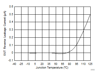
| Ilkg(OUT) | Reverse leakage current on OUT pin | VOUT = 6.5 V, VIN = VEN = 0 V, –40°C ≤ TJ ≤ 85°C, measure I(OUT) | 2 | µA | ||
| OUT - DISCHARGE | ||||||
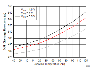
| R(DCHG) | OUT discharge resistance | 400 | 500 | 630 | Ω | |
| EN, CTL1, CTL2, CTL3 INPUTS | ||||||
| Input pin rising logic threshold voltage | 1 | 1.35 | 2 | V | ||
| Input pin falling logic threshold voltage | 0.85 | 1.15 | 1.65 | V | ||
| Hysteresis(2) | 200 | mV | ||||
| Input current | Pin voltage = 0 V or 6.5 V | –1 | 1 | µA | ||
| CURRENT LIMIT | ||||||
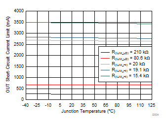
| IOS | OUT short-circuit current limit | R(ILIM_LO) = 210 kΩ | 205 | 255 | 305 | mA |
| R(ILIM_LO) = 80.6 kΩ | 600 | 660 | 720 | |||
| R(ILIM_LO) = 23.2 kΩ | 2145 | 2300 | 2455 | |||
| R(ILIM_HI) = 20 kΩ | 2500 | 2670 | 2840 | |||
| R(ILIM_HI) = 19.1 kΩ | 2620 | 2800 | 2975 | |||
| R(ILIM_HI) = 15.4 kΩ | 3255 | 3470 | 3685 | |||
| R(ILIM_HI) shorted to GND | 5500 | 7000 | 8000 | |||
| SUPPLY CURRENT | ||||||
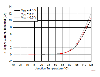
| I(IN_OFF) | Disabled IN supply current | V(EN) = 0 V, V(OUT) = 0 V, –40°C ≤ TJ ≤ 85°C | 0.1 | 5 | µA | |
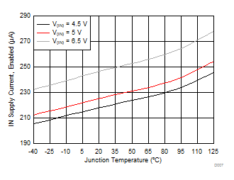
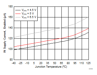
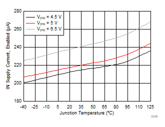
| I(IN_ON) | Enabled IN supply current | V(CTL)1 = V(CTL2) = V(CTL3) = V(IN) | 220 | 300 | µA | |
| V(CTL1) = V(CTL2) = 0 V, V(CTL3) = V(IN) | 226 | 300 | ||||
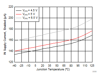
| V(CTL2) = V(IN), V(CTL1) = V(CTL3) = 0 V | 150 | 220 | ||||
| V(CTL1) = V(IN), V(CTL2) = V(CTL3) = 0 V | 115 | 190 | ||||
| UNDERVOLTAGE LOCKOUT, IN | ||||||
| V(UVLO) | IN rising UVLO threshold voltage | 3.9 | 4.1 | 4.3 | V | |
| Hysteresis(3) | TJ = 25°C | 100 | mV | |||
| FAULT | ||||||
| Output low voltage | I(FAULT) = 1 mA | 100 | mV | |||
| Off-state leakage | V(FAULT) = 6.5 V | 2 | µA | |||
| STATUS | ||||||
| Output low voltage | I(STATUS) = 1 mA | 100 | mV | |||
| Off-state leakage | V(STATUS) = 6.5 V | 2 | µA | |||
| THERMAL SHUTDOWN | ||||||
| T(OTSD2) | Thermal shutdown threshold | 155 | °C | |||
| T(OTSD1) | Thermal shutdown threshold in current-limit | 135 | °C | |||
| Hysteresis(3) | 20 | °C | ||||
| LOAD DETECT (VCTL1 = VCTL2 = VCTL3 = VIN) | ||||||
| I(LD) | IOUT load detection threshold | R(ILIM_LO) = 80.6 kΩ, rising load current | 630 | 700 | 770 | mA |
| Hysteresis(3) | 50 | mA | ||||
| DP_IN AND DM_IN SHORT-TO-VBUS PROTECTION | ||||||
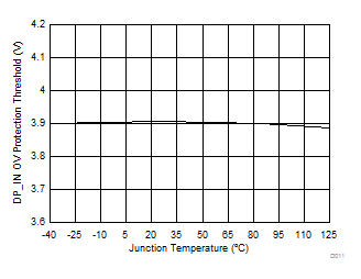
| V(OV) | Overvoltage protection trip threshold | DP_IN and DM_IN rising | 3.7 | 3.9 | 4.15 | V |
| Hysteresis(3) | 100 | mV | ||||
| R(DCHG_Data) | Discharge resistance after OVP | V(DP_IN) = V(DM_IN) = 5 V | 160 | 210 | 240 | kΩ |
| CABLE COMPENSATION | ||||||
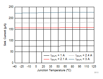
| I(CS) | Sink current | Load = 3 A, 2.5 V ≤ V(CS) ≤ 6.5 V | 214 | 225 | 236 | µA |
| Load = 2.4 A, 2.5 V ≤ V(CS) ≤ 6.5 V | 171 | 180 | 189 | |||
| Load = 2.1 A, 2.5 V ≤ V(CS) ≤ 6.5 V | 149 | 158 | 166 | |||
| Load = 1 A, 2.5 V ≤ V(CS) ≤ 6.5 V | 70 | 75 | 80 | |||
| HIGH-BANDWIDTH ANALOG SWITCH | ||||||
| R(HS_ON) | DP and DM switch on-resistance | V(DP_OUT) = V(DM_OUT) = 0 V, I(DP_IN) = I(DM_IN) = 30 mA | 2 | 4 | Ω | |
| V(DP_OUT) = V(DM_OUT) = 2.4 V, I(DP_IN) = I(DM_IN) = –15 mA | 2.9 | 6 | ||||
| |ΔR(HS_ON)| | Switch resistance mismatch between DP and DM channels | V(DP_OUT) = V(DM_OUT) = 0 V, I(DP_IN) = I(DM_IN) = 30 mA | 0.05 | 0.15 | Ω | |
| V(DP_OUT) = V(DM_OUT) = 2.4 V, I(DP_IN) = I(DM_IN) = –15 mA | 0.05 | 0.15 | ||||
| C(IO_OFF) | DP/DM switch off-state capacitance(4) | VEN = 0 V, V(DP_IN) = V(DM_IN) = 0.3 V, Vac = 0.03 VPP , f = 1 MHz |
6.7 | pF | ||
| C(IO_ON) | DP/DM switch on-state capacitance(4) | V(DP_IN) = V(DM_IN) = 0.3 V, Vac = 0.03 VPP, f = 1 MHz |
10 | pF | ||
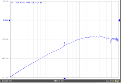
| Off-state isolation(4) | VEN = 0 V, f = 250 MHz | 27 | dB | |||
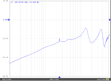
| On-state cross-channel isolation(4) | f = 250 MHz | 23 | dB | |||
| Ilkg(OFF) | Off-state leakage current, DP_OUT and DM_OUT | VEN = 0 V, V(DP_IN) = V (DM_IN) = 3.6 V, V(DP_OUT) = V(DM_OUT) = 0 V | 0.1 | 1.5 | µA | |
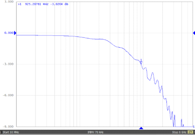
| BW | Bandwidth (–3 dB)(4) | R(L) = 50 Ω | 925 | MHz | ||
| CHARGING DOWNSTREAM PORT DETECT | ||||||
| V(DM_SRC) | DM_IN CDP output voltage | V(DP_IN) = 0.6 V, –250 µA < I(DM_IN) < 0 µA | 0.5 | 0.6 | 0.7 | V |
| V(DAT_REF) | DP_IN rising lower window threshold for VDM_SRC activation | 0.36 | 0.4 | V | ||
| Hysteresis(4) | 50 | mV | ||||
| V(LGC_SRC) | DP_IN rising upper window threshold for VDM_SRC de-activation | 0.8 | 0.88 | V | ||
| V(LGC_SRC_HYS) | Hysteresis(4) | 100 | mV | |||
| I(DP_SINK) | DP_IN sink current | V(DP_IN) = 0.6 V | 40 | 75 | 100 | µA |
| BC1.2 DCP MODE | ||||||
| R(DPM_SHORT) | DP_IN and DM_IN shorting resistance | 125 | 200 | Ω | ||
| DIVIDER3 MODE | ||||||
| V(DP_DIV3) | DP_IN output voltage | 2.57 | 2.7 | 2.84 | V | |
| V(DM_DIV3) | DM_IN output voltage | 2.57 | 2.7 | 2.84 | V | |
| R(DP_DIV3) | DP_IN output impedance | I(DP_IN) = –5 µA | 24 | 30 | 36 | kΩ |
| R(DM_DIV3) | DM_IN output impedance | I(DM_IN) = –5 µA | 24 | 30 | 36 | kΩ |
| 1.2-V MODE | ||||||
| V(DP_1.2V) | DP_IN output voltage | 1.12 | 1.2 | 1.26 | V | |
| V(DM_1.2V) | DM_IN output voltage | 1.12 | 1.2 | 1.26 | V | |
| R(DP_1.2V) | DP_IN output impedance | I(DP_IN) = –5 µA | 84 | 100 | 126 | kΩ |
| R(DM_1.2V) | DM_IN output impedance | I(DM_IN = –5 µA | 84 | 100 | 126 | |
(1) Pulse-testing techniques maintain junction temperature close to ambient temperature. Thermal effects must be taken into account separately.
(2) These parameters are provided for reference only and do not constitute part of TI's published device specifications for purposes of TI's product warranty.
(3) These parameters are provided for reference only and do not constitute part of TI's published device specifications for purposes of TI's product warranty.
(4) These parameters are provided for reference only and do not constitute part of TI's published device specifications for purposes of TI's product warranty.
6.6 Switching Characteristics
Unless otherwise noted –40°C ≤ TJ ≤ 125°C and 4.5 V ≤ V(IN) ≤ 6.5 V, V(EN) = V(IN), V(CTL1) = V(CTL2) = V(CTL3) = V(IN). R(FAULT) = R(STATUS) = 10 kΩ, R(ILIM_HI) = 19.1 kΩ, R(ILIM_LO) = 80.6 kΩ. Positive current is into pins. Typical value is at 25°C. All voltages are with respect to GND.| PARAMETER | TEST CONDITIONS | MIN | TYP | MAX | UNIT | |
|---|---|---|---|---|---|---|
| tr | OUT voltage rise time | V(IN) = 5 V, C(L) = 1 µF, R(L) = 100 Ω (see Figure 32 and Figure 33) | 0.7 | 1.14 | 2 | ms |
| tf | OUT voltage fall time | 0.2 | 0.35 | 0.6 | ms | |
| ton | OUT voltage turnon time | V(IN) = 5 V, C(L) = 1 µF, R(L) = 100 Ω (see Figure 32 andFigure 35) | 4.15 | 6 | ms | |
| toff | OUT voltage turnoff time | 1.8 | 3 | ms | ||
| t(DCHG_L) | Long OUT discharge hold time (SDP, CDP, or client mode to DCP_Auto) | Time V(OUT) < 0.7 V (see Figure 34) | 1.1 | 2 | 2.9 | s |
| t(DCHG_S) | Short OUT discharge hold time (DCP_Auto to SDP, CDP, or client mode) | Time V(OUT) < 0.7 V (see Figure 34) | 186 | 320 | 450 | ms |
| t(IOS) | OUT short-circuit response time(1) | V(IN) = 5 V, R(SHORT) = 50 mΩ (see Figure 25) | 2 | µs | ||
| t(OC_OUT_FAULT) | OUT FAULT deglitch time | Bidirectional deglitch applicable to current limit condition only (no deglitch assertion for OTSD) | 5.5 | 8 | 11.5 | ms |
| tpd | Analog switch propagation delay (1) | V(IN) = 5 V | 0.14 | ns | ||
| t(SK) | Analog switch skew between opposite transitions of the same port (tPHL – tPLH) (1) | V(IN) = 5 V | 0.02 | ns | ||
| t(LD_SET) | Load-detect set time | V(IN) = 5 V (See Figure 27) | 120 | 210 | 280 | ms |
| t(LD_RESET) | Load-detect reset time | V(IN) = 5 V (See Figure 28) | 1.8 | 3 | 4.2 | s |
| t(OV_D) | DP_IN and DM_IN over-voltage protection response time | V(OUT) = 5 V (See Figure 29) | 2 | µs | ||
| t(OV_D_FAULT) | DP_IN and DM_IN FAULT degltich time | V(OUT) = 5 V (See Figure 30) | 11 | 16 | 23 | ms |
(1) These parameters are provided for reference only and do not constitute part of TI's published device specifications for purposes of TI's product warranty.
6.7 Typical Characteristics

| VIN = 5 V |
| VIN = 5 V |
| A |
| CTL1 = 1 | CTL2 = 1 | CTL3 = 1 |
| CTL1 = 0 | CTL2 = 0 | CTL3 = 1 |
| CTL1 = 1 | CTL2 = 0 | CTL3 = 0 |
| VIN = 5 V |
| VIN = 5 V | VCS = 2. 5 V |
| VIN = 5 V |
| CTL1 = 1 | CTL2 = 1 | CTL3 = 1 |
| CTL1 = 0 | CTL2 = 1 | CTL3 = 0 |
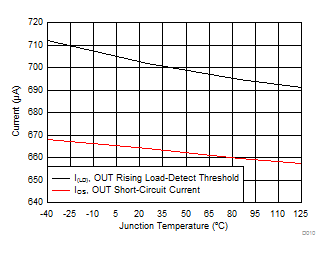
| R(ILIM_LO) = 80.6 kΩ |
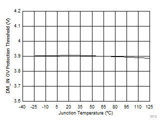
| VIN = 5 V |
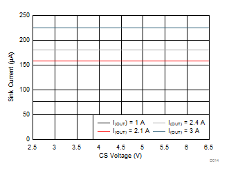
| VIN = 6.5 V |
Forcing a page break between ImageMatrices
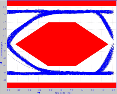
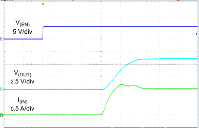
| R(LOAD) = 5 Ω | C(LOAD) = 150 µF | t = 1 ms/div |
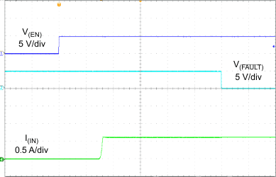
| R(ILIM_HI) = 80.6 kΩ | t = 2 ms/div |
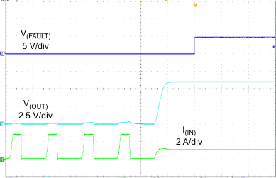
| R(ILIM_HI) = 19.1 kΩ | t = 4 ms/div |
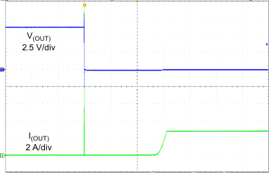
| R(ILIM_HI) = 19.1 kΩ | R(SHORT) = 50 mΩ | t = 1 ms/div |
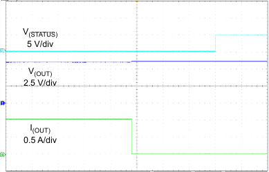
| R(ILIM_LO) = 80.6 kΩ | t = 1 s/div |
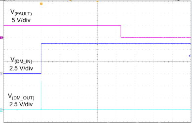
| R(DM_OUT) = 15 kΩ | t = 4 ms/div |
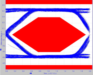
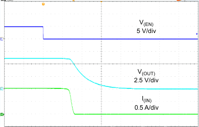
| R(LOAD) = 5 Ω | C(LOAD) = 150 µF | t = 1 ms/div |
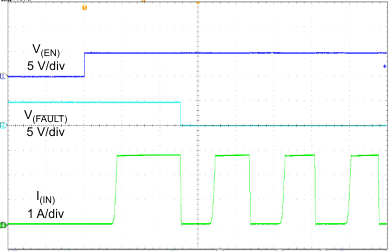
| R(ILIM_HI) = 19.1 kΩ | t = 4 ms/div |
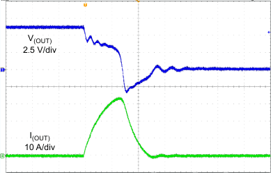
| R(SHORT) = 50 mΩ | t = 1 µs/div |
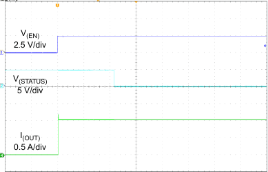
| R(ILIM_LO) = 80.6 kΩ | t = 100 ms/div |
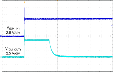
| R(DM_OUT) = 15 kΩ | t = 1 µs/div |
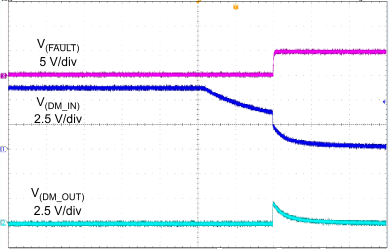
| R(DM_OUT) = 15 kΩ | t = 1 µs/div |