ZHCSA62B August 2012 – August 2014 TPS22965
PRODUCTION DATA.
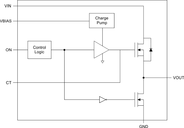
8 Detailed Description
8.1 Overview
The device is a single channel, 6-A load switch in an 8-terminal SON package. To reduce the voltage drop in high current rails, the device implements an ultra-low resistance N-channel MOSFET. The device has a programmable slew rate for applications that require specific rise-time.
The device has very low leakage current during off state. This prevents downstream circuits from pulling high standby current from the supply. Integrated control logic, driver, power supply, and output discharge FET eliminates the need for any external components, which reduces solution size and bill of materials (BOM) count.
8.2 Functional Block Diagram
8.3 Feature Description
8.3.1 Adjustable Rise Time
A capacitor to GND on the CT terminal sets the slew rate. The voltage on the CT terminal can be as high as 12 V. Therefore, the minimum voltage rating for the CT cap should be 25 V for optimal performance. An approximate formula for the relationship between CT and slew rate when VBIAS is set to 5 V is shown in Equation 1 below. This equation accounts for 10% to 90% measurement on VOUT and does NOT apply for CT = 0 pF. Use table below to determine rise times for when CT = 0 pF.
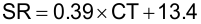
Where,
SR = slew rate (in µs/V)
CT = the capacitance value on the CT terminal (in pF)
The units for the constant 13.4 are µs/V. The units for the constant 0.39 are µs/(V*pF).
Rise time can be calculated by multiplying the input voltage by the slew rate. The table below contains rise time values measured on a typical device. Rise times shown below are only valid for the power-up sequence where VIN and VBIAS are already in steady state condition before the ON terminal is asserted high.
Table 1. Rise Time vs CT Capacitor
| CT (pF) | RISE TIME (µs) 10% - 90%, CL = 0.1 µF, CIN = 1 µF, RL = 10 Ω, VBIAS = 5 V TYPICAL VALUES at 25°C with a 25V X7R 10% CERAMIC CAPACITOR on CT |
||||||
|---|---|---|---|---|---|---|---|
| VIN = 5 V | VIN = 3.3 V | VIN = 1.8 V | VIN = 1.5 V | VIN = 1.2 V | VIN = 1.05 V | VIN = 0.8 V | |
| 0 | 127 | 93 | 62 | 55 | 51 | 46 | 42 |
| 220 | 475 | 314 | 188 | 162 | 141 | 125 | 103 |
| 470 | 939 | 637 | 359 | 304 | 255 | 218 | 188 |
| 1000 | 1869 | 1229 | 684 | 567 | 476 | 414 | 344 |
| 2200 | 4020 | 2614 | 1469 | 1211 | 1024 | 876 | 681 |
| 4700 | 8690 | 5746 | 3167 | 2703 | 2139 | 1877 | 1568 |
| 10000 | 18360 | 12550 | 6849 | 5836 | 4782 | 4089 | 3449 |
8.3.2 Quick Output Discharge
The TPS22965 includes a Quick Output Discharge (QOD) feature. When the switch is disabled, a discharge resistor is connected between VOUT and GND. This resistor has a typical value of 225-Ω and prevents the output from floating while the switch is disabled.
8.3.3 Low Power Consumption During Off State
The ISD VIN supply current is 0.01-µA typical at 1.8-VIN. Typically, the downstream loads would have a significantly higher off-state leakage current. The load switch allows system standby power consumption to be reduced.
8.4 Device Functional Modes
Table 2. Functional Table
| ON | VIN to VOUT | VOUT to GND |
|---|---|---|
| L | Off | On |
| H | On | Off |