ZHCSUV3E April 2009 – April 2024 TPS22960
PRODUCTION DATA
- 1
- 1 特性
- 2 应用
- 3 说明
- 4 Pin Configuration and Functions
- 5 Specifications
- 6 Parameter Measurement Information
- 7 Detailed Description
- 8 Application and Implementation
- 9 Device and Documentation Support
- 10Revision History
- 11Mechanical, Packaging, and Orderable Information
封装选项
机械数据 (封装 | 引脚)
散热焊盘机械数据 (封装 | 引脚)
- DCN|8
订购信息
5.8 Typical Switching Characteristics
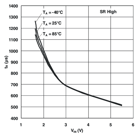 Figure 5-6 Rise Time vs Input Voltage
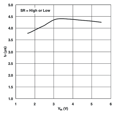 Figure 5-8 Fall Time vs Input Voltage
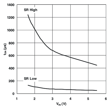 Figure 5-10 On Time vs Input Voltage
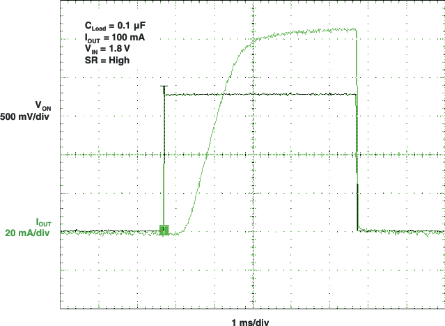 Figure 5-12 tON Response
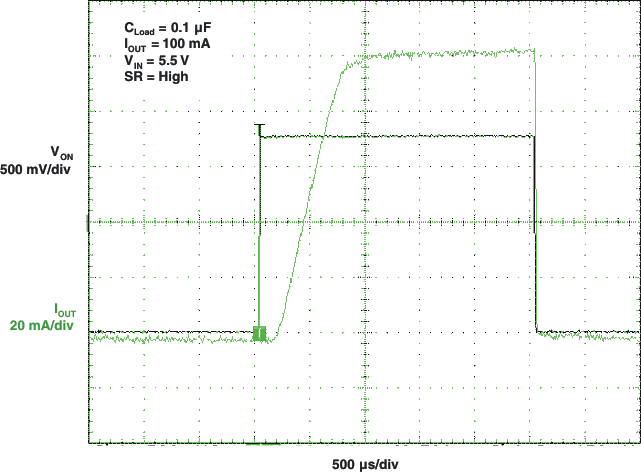 Figure 5-14 tON Response
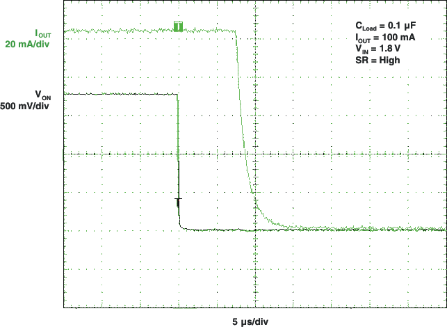 Figure 5-16 tOFF Response
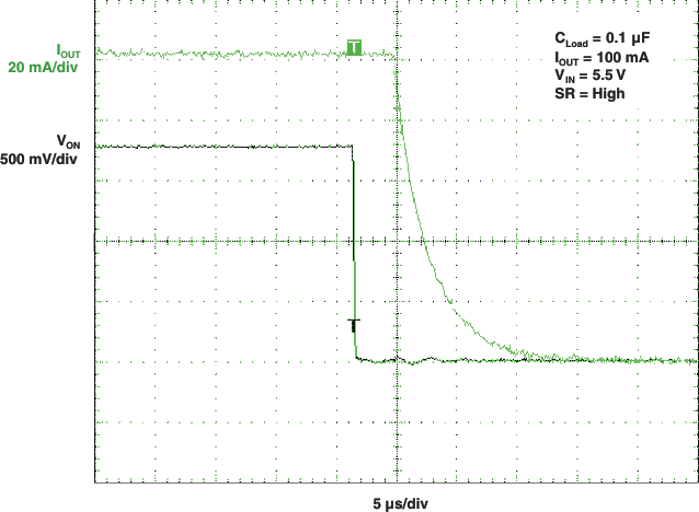 Figure 5-18 tOFF Response
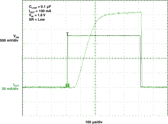 Figure 5-20 tON Response
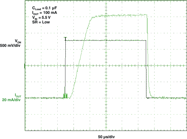 Figure 5-22 tON Response
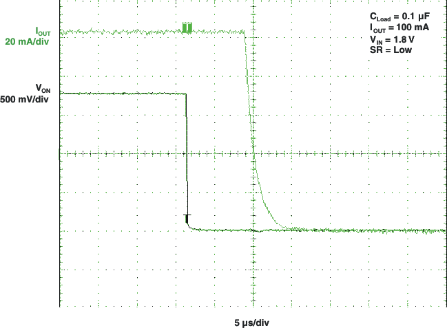 Figure 5-24 tOFF Response
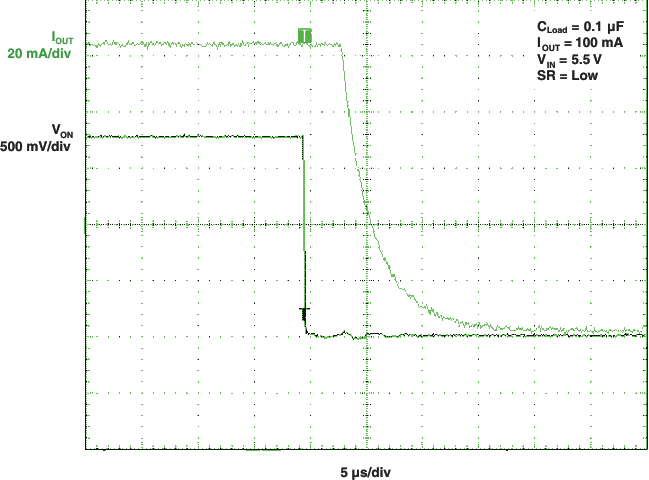 Figure 5-26 tOFF Response
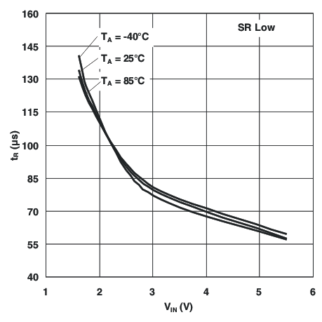 Figure 5-7 Rise Time vs Input Voltage
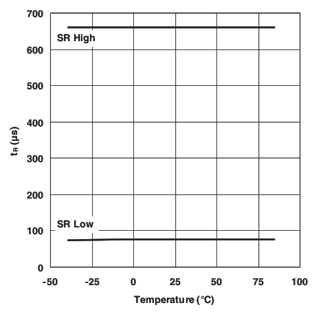 Figure 5-9 Rise Time vs Temperature
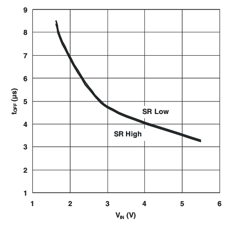 Figure 5-11 Off Time vs Input Voltage
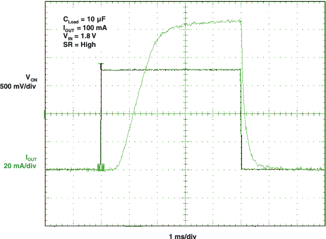 Figure 5-13 tON Response
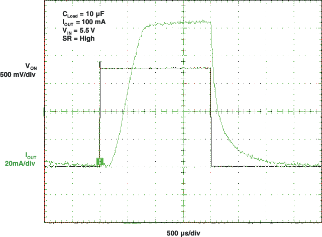 Figure 5-15 tON Response
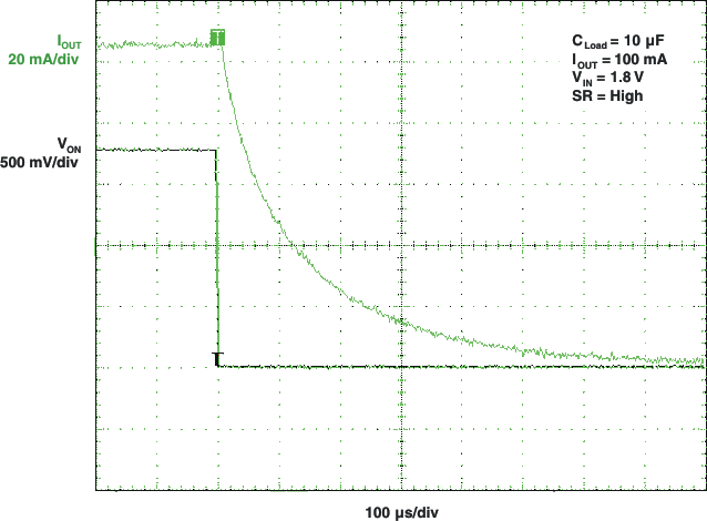 Figure 5-17 tOFF Response
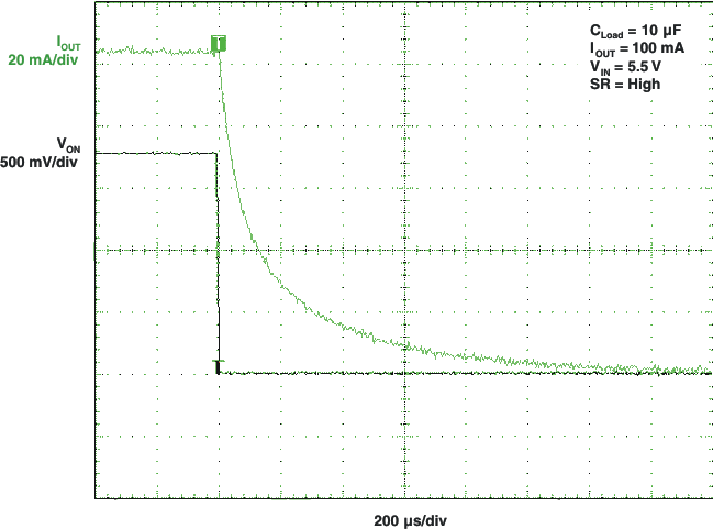 Figure 5-19 tOFF Response
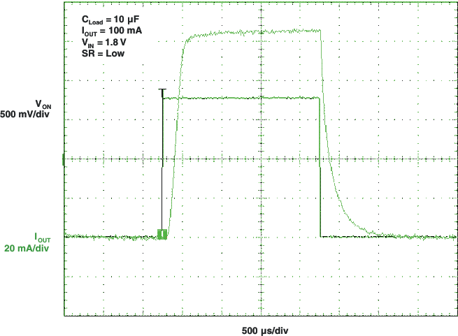 Figure 5-21 tON Response
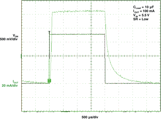 Figure 5-23 tON Response
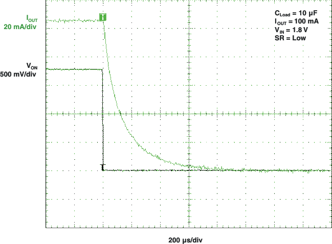 Figure 5-25 tOFF Response
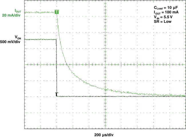 Figure 5-27 tOFF Response