ZHCSEX7C November   2015  – February 2016 TPS22925

PRODUCTION DATA.  

  1. 特性
  2. 应用
  3. 说明
  4. 修订历史记录
  5. Device Comparison Table
  6. Pin Configuration and Functions
  7. Specifications
    1. 7.1 Absolute Maximum Ratings
    2. 7.2 ESD Ratings
    3. 7.3 Recommended Operating Conditions
    4. 7.4 Thermal Information
    5. 7.5 Electrical Characteristics
    6. 7.6 Switching Characteristics
    7. 7.7 Typical Characteristics
  8. Detailed Description
    1. 8.1 Overview
    2. 8.2 Functional Block Diagram
    3. 8.3 Feature Description
      1. 8.3.1 ON and OFF Control
      2. 8.3.2 Quick Output Discharge (QOD) (TPS22925B and TPS22925C only)
      3. 8.3.3 Reverse Current Blocking
    4. 8.4 Device Functional Modes
  9. Application and Implementation
    1. 9.1 Application Information
      1. 9.1.1 VIN to VOUT Voltage Drop
      2. 9.1.2 Input Capacitor (CIN)
      3. 9.1.3 Load Capacitor (CL)
      4. 9.1.4 Standby Power Reduction
      5. 9.1.5 Power Multiplexing
      6. 9.1.6 Thermal Considerations
    2. 9.2 Typical Application
      1. 9.2.1 Design Requirements
      2. 9.2.2 Detailed Design Procedure
        1. 9.2.2.1 Managing Inrush Current
      3. 9.2.3 Application Curve
  10. 10Power Supply Recommendations
  11. 11Layout
    1. 11.1 Layout Guidelines
    2. 11.2 Layout Example
  12. 12器件和文档支持
    1. 12.1 社区资源
    2. 12.2 商标
    3. 12.3 静电放电警告
    4. 12.4 Glossary
  13. 13机械、封装和可订购信息

封装选项

机械数据 (封装 | 引脚)
散热焊盘机械数据 (封装 | 引脚)
订购信息

11 Layout

11.1 Layout Guidelines

For best performance, all traces should be as short as possible. To be most effective, the input and load capacitors should be placed close to the device to minimize the effects that parasitic trace inductances may have on operation. Using wide traces for VIN, VOUT, and GND helps minimize the parasitic electrical effects.

11.2 Layout Example
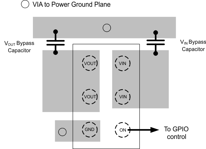
TPS22925 layout_slvs840.gif Figure 35. TPS22925xx Layout Example