SLVS749C November 2008 – January 2015 TPS22921 , TPS22922
UNLESS OTHERWISE NOTED, this document contains PRODUCTION DATA.
- 1 Features
- 2 Applications
- 3 Description
- 4 Typical Application
- 5 Revision History
- 6 Device Comparison Table
- 7 Pin Configuration and Functions
-
8 Specifications
- 8.1 Absolute Maximum Ratings
- 8.2 ESD Ratings
- 8.3 Recommended Operating Conditions
- 8.4 Thermal Information
- 8.5 Electrical Characteristics
- 8.6 Switching Characteristics: VIN = 0.9 V
- 8.7 Switching Characteristics: VIN = 1 V
- 8.8 Switching Characteristics: VIN = 1.1 V
- 8.9 Switching Characteristics: VIN = 1.2 V
- 8.10 Switching Characteristics: VIN = 1.8 V
- 8.11 Switching Characteristics: VIN = 2.5 V
- 8.12 Switching Characteristics: VIN = 3 V
- 8.13 Switching Characteristics: VIN = 3.6 V
- 8.14
Typical Characteristics
- 8.14.1 Typical DC Characteristics
- 8.14.2 Typical AC Characteristics (TPS22921)
- 8.14.3 Typical AC Characteristics (TPS22922)
- 8.14.4 Typical AC Characteristics (TPS22922B)
- 8.14.5 Typical AC Characteristics (TPS22921 and TPS22922)
- 8.14.6 Typical AC Characteristics (TPS22921)
- 8.14.7 Typical AC Characteristics (TPS22922)
- 8.14.8 Typical AC Characteristics (TPS22922B)
- 9 Parameter Measurement Information
- 10Detailed Description
- 11Application and Implementation
- 12Power Supply Recommendations
- 13Layout
- 14Device and Documentation Support
- 15Mechanical, Packaging, and Orderable Information
13 Layout
13.1 Layout Guidelines
For best performance, VIN, VOUT, and GND traces should be as short and wide as possible to help minimize the parasitic electrical effects. To be most effective, the input and output capacitors should be placed close to the device to minimize the effects that parasitic trace inductances may have on normal operation.
For higher reliability, the maximum IC junction temperature, TJ(max), should be restricted to 125˚C under normal operating conditions. Junction temperature is directly proportional to power dissipation in the device and the two are related by
Equation 5. TJ = TA + θJA × PD
where
- TJ = Junction temperature of the device
- TA = Ambient temperature
- PD = Power dissipation inside the device
- θJA = Junction to ambient thermal resistance. See Thermal Information section of the data sheet. This parameter is highly dependent on board layout.
13.2 Layout Example
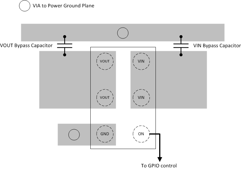 Figure 55. Layout Recommendation