SLVSAY8D June 2011 – January 2016 TPS22920
PRODUCTION DATA.
- 1 Features
- 2 Applications
- 3 Description
- 4 Revision History
- 5 Device Comparison Table
- 6 Pin Configuration and Functions
-
7 Specifications
- 7.1 Absolute Maximum Ratings
- 7.2 ESD Ratings
- 7.3 Recommended Operating Conditions
- 7.4 Thermal Information
- 7.5 Electrical Characteristics
- 7.6 Switching Characteristics: VIN = 3.6 V
- 7.7 Switching Characteristics: VIN = 0.9 V
- 7.8 Typical DC Characteristics
- 7.9 TPS22920 Typical AC Characteristics
- 7.10 TPS22920L Typical AC Characteristics
- 8 Parametric Measurement Information
- 9 Detailed Description
- 10Application and Implementation
- 11Power Supply Recommendations
- 12Layout
- 13Device and Documentation Support
- 14Mechanical, Packaging, and Orderable Information
9 Detailed Description
9.1 Overview
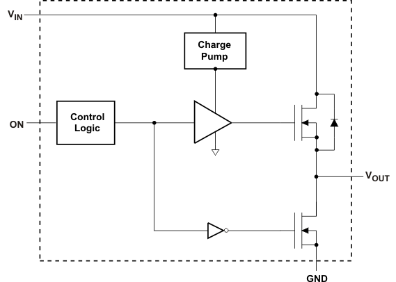
The TPS22920x is a single channel, 4-A load switch in a small, space-saving CSP-8 package. This device implements a low resistance N-channel MOSFET with a controlled rise time for applications that need to limit the inrush current.
This device is also designed to have very low leakage current during off state, which prevents downstream circuits from pulling high standby current from the supply. Integrated control logic, driver, power supply, and output discharge FET eliminates the need for additional external components, which reduces solution size and bill of materials (BOM) count.
9.2 Functional Block Diagram

9.3 Feature Description
9.3.1 ON/OFF Control
The ON pin controls the state of the switch. For TPS22920, asserting ON high enables the switch. For TPS22920L, asserting ON low enables the switch. ON has a low threshold, making it capable of interfacing with low-voltage signals. The ON pin is compatible with standard GPIO logic threshold. It can be used with any microcontroller with 1.2-V, 1.8-V, 2.5-V or 3.3-V GPIOs.
9.3.2 Output Pull-Down
The output pull-down is active when the user is turning off the main pass FET. The pull-down discharges the output rail to approximately 10% of the rail, and then the output pull-down is automatically disconnected to optimize the shutdown current.
9.4 Device Functional Modes
| ON | TPS22920 | TPS22920L | ||
|---|---|---|---|---|
| VIN to VOUT | VOUT to GND(1) | VIN to VOUT | VOUT to GND(1) | |
| Logic Low | OFF | ON | ON | OFF |
| Logic High | ON | OFF | OFF | ON |