ZHCSHY9 April   2018 TPS22810-Q1

PRODUCTION DATA.  

  1. 特性
  2. 应用
  3. 说明
    1.     简化原理图
  4. 修订历史记录
  5. Pin Configuration and Functions
    1.     Pin Functions
  6. Specifications
    1. 6.1 Absolute Maximum Ratings
    2. 6.2 ESD Ratings
    3. 6.3 Recommended Operating Conditions
    4. 6.4 Thermal Information
    5. 6.5 Electrical Characteristics
    6. 6.6 Switching Characteristics
    7. 6.7 Typical DC Characteristics
    8. 6.8 Typical AC Characteristics
  7. Parameter Measurement Information
  8. Detailed Description
    1. 8.1 Overview
    2. 8.2 Functional Block Diagram
    3. 8.3 Feature Description
      1. 8.3.1 On and Off Control
      2. 8.3.2 Quick Output Discharge (QOD)
        1. 8.3.2.1 QOD when System Power is Removed
        2. 8.3.2.2 Internal QOD Considerations
      3. 8.3.3 EN/UVLO
      4. 8.3.4 Adjustable Rise Time (CT)
      5. 8.3.5 Thermal Shutdown
    4. 8.4 Device Functional Modes
  9. Application and Implementation
    1. 9.1 Application Information
      1. 9.1.1 ON and OFF Control
      2. 9.1.2 Input Capacitor (Optional)
      3. 9.1.3 Output Capacitor (Optional)
    2. 9.2 Typical Application
      1. 9.2.1 Design Requirements
      2. 9.2.2 Detailed Design Procedure
        1. 9.2.2.1 Shutdown Sequencing During Unexpected Power Loss
        2. 9.2.2.2 VIN to VOUT Voltage Drop
        3. 9.2.2.3 Inrush Current
      3. 9.2.3 Application Curves
  10. 10Power Supply Recommendations
  11. 11Layout
    1. 11.1 Layout Guidelines
    2. 11.2 Layout Example
    3. 11.3 Thermal Considerations
  12. 12器件和文档支持
    1. 12.1 器件支持
      1. 12.1.1 开发支持
    2. 12.2 文档支持
      1. 12.2.1 相关文档
    3. 12.3 接收文档更新通知
    4. 12.4 社区资源
    5. 12.5 商标
    6. 12.6 静电放电警告
    7. 12.7 Glossary
  13. 13机械、封装和可订购信息

封装选项

机械数据 (封装 | 引脚)
散热焊盘机械数据 (封装 | 引脚)
订购信息

Application Curves

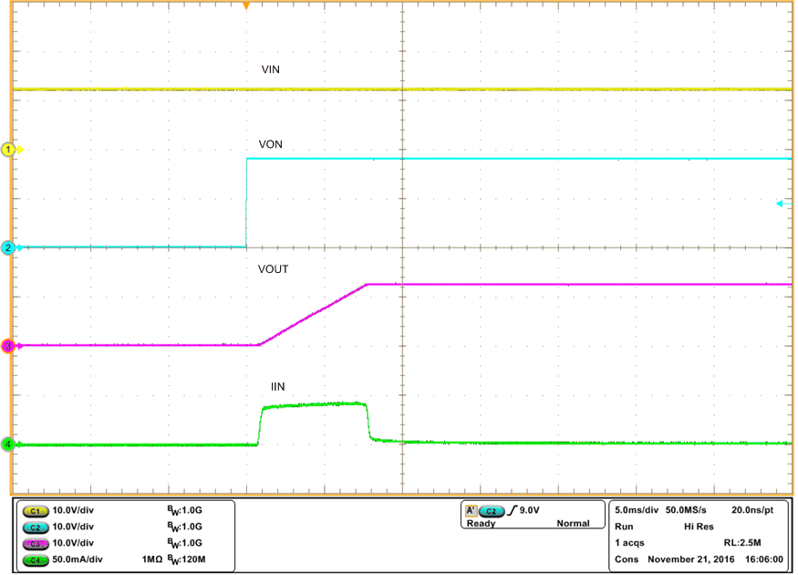
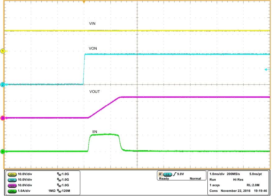
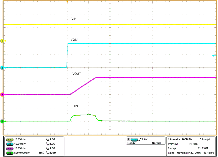
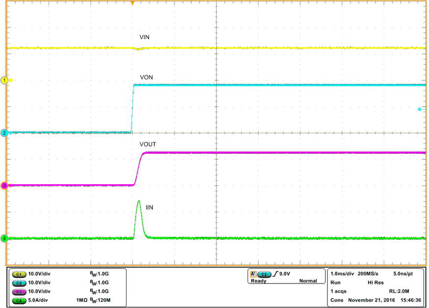
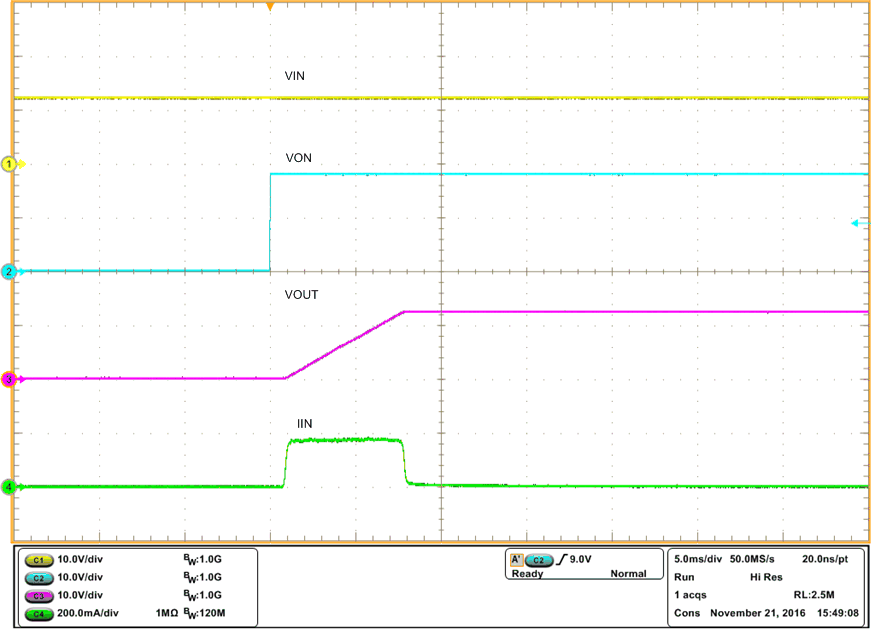
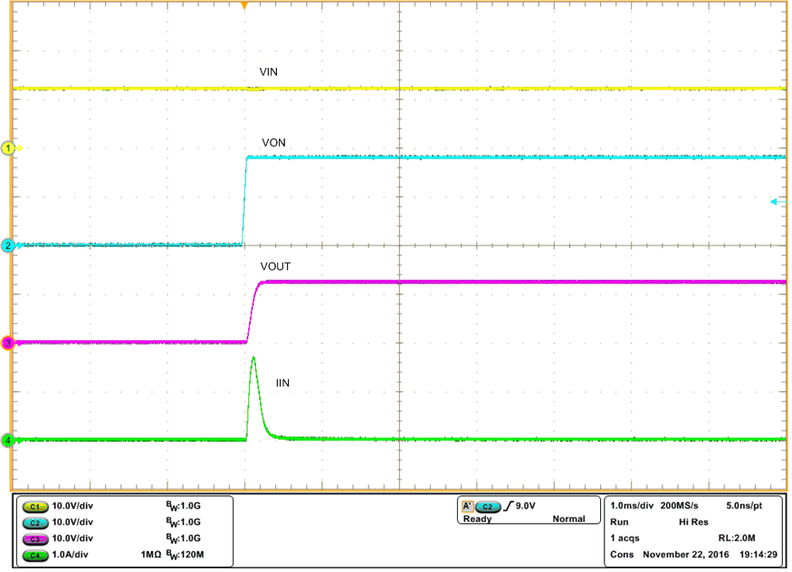
See the oscilloscope captures below for an example of how the CT capacitor can be used to reduce inrush current for VIN = 12 V. See the Adjustable Rise Time (CT) section for rise times for corresponding CT values.
TPS22810-Q1 tps22810_Fig35_VIN_12V_CT_0pF_CIN_1.gif
Figure 28. TPS22810-Q1 Inrush Current With
CL = 22 µF, CT = 0 pF
TPS22810-Q1 tps22810_Fig37_VIN_12V_CT_27000pF_C.gif
Figure 30. TPS22810-Q1 Inrush Current
With CL = 22 µF, CT = 27000 pF
TPS22810-Q1 tps22810_Fig39_VIN_12V_CT_4700pF_CI.gif
Figure 32. TPS22810-Q1 Inrush Current
With CL = 100 µF, CT = 4700 pF
TPS22810-Q1 tps22810_Fig36_VIN_12V_CT_4700pF_CI.gif
Figure 29. TPS22810-Q1 Inrush Current
with CL = 22 µF, CT = 4700 pF
TPS22810-Q1 tps22810_Fig38_VIN_12V_CT_0pF_COUT_.gif
Figure 31. TPS22810-Q1 Inrush Current
With CL = 100 µF, CT = 0 pF
TPS22810-Q1 tps22810_Fig38_VIN_12V_CT_27000pF_C.gif
Figure 33. TPS22810-Q1 Inrush Current
With CL = 100 µF, CT = 27000 pF