ZHCSFH0 September 2016 TPL5010-Q1
PRODUCTION DATA.
- 1 特性
- 2 应用
- 3 说明
- 4 修订历史记录
- 5 器件比较表
- 6 Pin Configuration and Functions
- 7 Specifications
- 8 Detailed Description
- 9 Application and Implementation
- 10Power Supply Recommendations
- 11Layout
- 12器件和文档支持
- 13机械、封装和可订购信息
8 Detailed Description
8.1 Overview
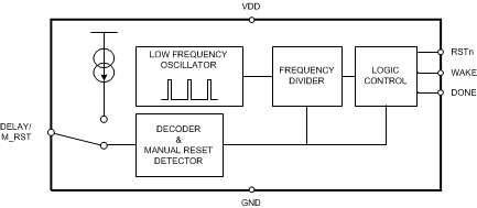
The TPL5010-Q1 is a system wakeup timer with a watchdog feature, ideal for low power applications. TPL5010-Q1 is ideal for use in interrupt-driven applications and provides selectable timing from 100 ms to 7200 s.
8.2 Functional Block Diagram

8.3 Feature Description
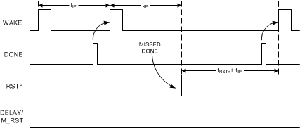
The DONE, WAKE and RSTn signals are used to implement the watchdog function. The TPL5010-Q1 is programmed to issue a periodic WAKE pulse to a µC which is in sleep or standby mode. After receiving the WAKE pulse, the µC must issue a DONE signal to the TPL5010-Q1 at least 20 ms before the rising edge of the next WAKE pulse. If the DONE signal is not asserted, the TPL5010-Q1 asserts the RSTn signal to reset the µC. A manual reset function is realized by momentarily pulling the DELAY/M_RST pin to VDD.
 Figure 8. Watchdog
8.3.1 WAKE
The WAKE pulse is sent out from the TPL5010-Q1 when the programmed time interval starts (except at the beginning of the first cycle or if in the previous interval the DONE has not been received).
This signal is normally low.
8.3.2 DONE
The DONE pin is driven by a µC to signal successful processing of the WAKE signal. The TPL5010-Q1 recognizes a valid DONE signal as a low to high transition; if two or more DONE signals are received within the time interval, only the first DONE signal is processed.
The DONE signal resets the counter of the watchdog only. If the DONE signal is received when the WAKE is still high, the WAKE will go low as soon as the DONE is recognized.
8.3.3 RSTn
To implement the reset interface between the TPL5010-Q1 and the µC a pull-up resistance is required. 100 kΩ is recommended, to minimize current.
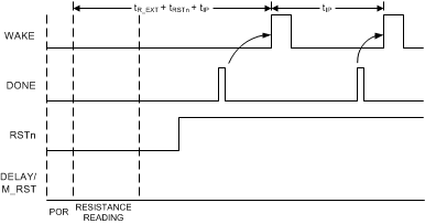
During the POR and the reading of the REXT the RSTn signal is LOW.
RSTn is asserted (LOW) for either one of the following conditions:
- 1. If the DELAY/M_RST pin is high for at least two consecutive cycles of the internal oscillator (approximately 20 ms).
- 2. At the beginning of a new time interval if DONE is not received at least 20 ms before the next WAKE rising edge (see Figure 8).
8.4 Device Functional Modes
8.4.1 Startup
During startup, after POR, the TPL5010-Q1 executes a one-time measurement of the resistance attached to the DELAY/M_RST pin in order to determine the desired time interval for WAKE. This measurement interval is tR_EXT. During this measurement a constant current is temporarily flowing into REXT.
 Figure 9. Startup
8.4.2 Normal Operating Mode
During normal operating mode, the TPL5010-Q1 asserts periodic WAKE pulses in response to valid DONE pulses from the µC. If either a manual reset is applied (logic HIGH on DELAY/M_RST pin) or the µC does not issue a DONE pulse within the required time, the TPL5010-Q1 asserts the RSTn signal to the µC and restarts its internal counters. See Figure 8 and Figure 10 .
8.5 Programming
8.5.1 Configuring the WAKE Interval with the DELAY/M_RST Pin
The time interval between 2 adjacent WAKE pulses (rising edges) is selectable through an external resistance (REXT) between the DELAY/M_RST pin and ground. The value of the resistance REXT is converted one time after POR. The allowable range of REXT is 500 Ω to 170 kΩ. At least a 1% precision resistance is recommended. See Timer Interval Selection Using External Resistance for how to set the WAKE pulse interval using REXT.
The time between 2 adjacent RESET signals (falling edges) or between a RESET (falling edge) and a WAKE (rising edge) is given by the sum of the programmed time interval and the tRSTn (reset pulse width).
8.5.2 Manual Reset
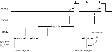
If VDD is connected to the DELAY/M_RST pin, the TPL5010-Q1 recognizes this as a manual reset condition. In this case the time interval is not set. If the manual reset is asserted during the POR or during the reading procedure, the reading procedure is aborted and is re-started as soon as the manual reset switch is released. A pulse on the DELAY/M_RST pin is recognized as a valid manual reset only if it lasts at least 20 ms (observation time is 30 ms).
A valid manual reset resets all the counters inside the TPL5010-Q1. The counters restart only when the high digital voltage at DELAY/M_RST is removed and the next tRSTn is elapsed.
 Figure 10. Manual Reset
8.5.2.1 DELAY/M_RST
A resistance in the range between 500 Ω and 170 kΩ needs to be connected in order to select a valid time interval. At the POR and during the reading of the resistance the DELAY/M_RST is connected to an analog signal chain though a mux. After the reading of the resistance the analog circuit is switched off and the DELAY/RST is connected to a digital circuit.
The manual reset detection is supported with a de-bounce feature which makes the TPL5010-Q1 insensitive to the glitches on the DELAY/M_RST pin. When a valid manual reset signal is asserted on the DELAY/M_RST pin, the RSTn signal is asserted LOW after a delay of tM_RST. It remains LOW after a valid manual reset is asserted + tDB + tRSTn. Due to the asynchronous nature of the manual reset signal and its arbitrary duration, the LOW status of the RSTn signal maybe affected by an uncertainty of about ±5 ms.
A valid manual reset puts all the digital output signals at their default values:
- WAKE = LOW
- RSTn = asserted LOW
8.5.2.2 Circuitry
The manual reset may be implemented using a switch (momentary mechanical action). The TPL5010-Q1 offers 2 possible approaches according to the power consumption constraints of the application.
 Figure 11. Manual Reset with SPST Switch
For use cases that do not require the lowest power consumption, using a single pole single throw switch may offer a lower cost solution. The DELAY/M_RST pin may be directly connected to VDD with REXT in the circuit. The current drawn from the supply voltage during the reset is given by VDD/REXT.
 Figure 12. Manual Reset with SPDT Switch
The reset function may also be asserted by switching DELAY/M_RST from REXT to VDD using a single pole double throw switch, which will provide a lower power solution for the manual reset, because no current flows.
8.5.3 Timer Interval Selection Using External Resistance
In order to set the time interval, the external resistance REXT is selected according the following formula:

where
- T is the desired time interval in seconds
- REXT is the resistance value to use in Ω
- a, b, c are coefficients depending on the range of the time interval
Table 2. Coefficients for Equation 1
| SET | TIME INTERVAL RANGE (s) | a | b | c |
|---|---|---|---|---|
| 1 | 1 < T ≤ 5 | 0.2253 | –20.7654 | 570.5679 |
| 2 | 5 < T ≤ 10 | –0.1284 | 46.9861 | –2651.8889 |
| 3 | 10 < T ≤ 100 | 0.1972 | –19.3450 | 692.1201 |
| 4 | 100 < T ≤ 1000 | 0.2617 | –56.2407 | 5957.7934 |
| 5 | T > 1000 | 0.3177 | –136.2571 | 34522.4680 |
EXAMPLE
Required time interval: 8 s
The coefficient set to be selected is the number 2. The formula becomes:

The resistance value is 10.18 kΩ.
Table 3 and Table 4 contain example values of tIP and their corresponding value of REXT.
Table 3. First 9 Time Intervals
| tIP (ms) | RESISTANCE (Ω) | CLOSEST REAL VALUE (Ω) | PARALLEL OF TWO 1% TOLERANCE RESISTORS (kΩ) |
|---|---|---|---|
| 100 | 500 | 500 | 1.0 // 1.0 |
| 200 | 1000 | 1000 | - |
| 300 | 1500 | 1500 | 2.43 // 3.92 |
| 400 | 2000 | 2000 | - |
| 500 | 2500 | 2500 | 4.42 // 5.76 |
| 600 | 3000 | 3000 | 5.36 // 6.81 |
| 700 | 3500 | 3500 | 4.75 // 13.5 |
| 800 | 4000 | 4000 | 6.19 // 11.3 |
| 900 | 4500 | 4501 | 6.19 // 16.5 |
Table 4. Most Common Time Intervals Between 1 s to 2 h
| tIP | CALCULATED RESISTANCE (kΩ) | CLOSEST REAL VALUE (kΩ) | PARALLEL OF TWO 1% TOLERANCE RESISTORS (kΩ) |
|---|---|---|---|
| 1 s | 5.20 | 5.202 | 7.15 // 19.1 |
| 2 s | 6.79 | 6.788 | 12.4 // 15.0 |
| 3 s | 7.64 | 7.628 | 12.7// 19.1 |
| 4 s | 8.30 | 8.306 | 14.7 // 19.1 |
| 5 s | 8.85 | 8.852 | 16.5 // 19.1 |
| 6 s | 9.27 | 9.223 | 18.2 // 18.7 |
| 7 s | 9.71 | 9.673 | 19.1 // 19.6 |
| 8 s | 10.18 | 10.180 | 11.5 // 8.87 |
| 9 s | 10.68 | 10.68 | 17.8 // 26.7 |
| 10 s | 11.20 | 11.199 | 15.0 // 44.2 |
| 20 s | 14.41 | 14.405 | 16.9 // 97.6 |
| 30 s | 16.78 | 16.778 | 32.4 // 34.8 |
| 40 s | 18.75 | 18.748 | 22.6 // 110.0 |
| 50 s | 20.047 | 20.047 | 28.7 // 66.5 |
| 1 min | 22.02 | 22.021 | 40.2 // 48.7 |
| 2 min | 29.35 | 29.349 | 35.7 // 165.0 |
| 3 min | 34.73 | 34.729 | 63.4 // 76.8 |
| 4 min | 39.11 | 39.097 | 63.4 // 102.0 |
| 5 min | 42.90 | 42.887 | 54.9 // 196.0 |
| 6 min | 46.29 | 46.301 | 75.0 // 121.0 |
| 7 min | 49.38 | 49.392 | 97.6 // 100.0 |
| 8 min | 52.24 | 52.224 | 88.7 // 127.0 |
| 9 min | 54.92 | 54.902 | 86.6 // 150.0 |
| 10 min | 57.44 | 57.437 | 107.0 // 124.0 |
| 20 min | 77.57 | 77.579 | 140.0 // 174.0 |
| 30 min | 92.43 | 92.233 | 182.0 // 187.0 |
| 40 min | 104.67 | 104.625 | 130.0 // 536.00 |
| 50 min | 115.33 | 115.331 | 150.0 // 499.00 |
| 1 h | 124.91 | 124.856 | 221.0 // 287.00 |
| 1 h 30 min | 149.39 | 149.398 | 165.0 // 1580.0 |
| 2 h | 170.00 | 170.00 | 340.0 // 340.0 |
8.5.4 Quantization Error
The TPL5010-Q1 can generate 1650 discrete timer intervals in the range of 100 ms to 7200 s. The first 9 intervals are multiples of 100 ms. The remaining 1641 intervals cover the range between 1 s to 7200 s. Because they are discrete intervals, there is a quantization error associated with each value.
The quantization error can be evaluated according to the following formula:

Where:


where
- REXT is the resistance calculated with Equation 1
- a, b, c are the coefficients of the equation listed in Table 2
8.5.5 Error Due to Real External Resistance
REXT is a theoretical value and may not be available in standard commercial resistor values. It is possible to closely approach the theoretical REXT using two or more standard values in parallel. However, standard values are characterized by a certain tolerance. This tolerance will affect the accuracy of the time interval.
The accuracy can be evaluated using the following procedure:
- Evaluate the min and max values of REXT (REXT_MIN, REXT_MAX with Equation 1 using the selected commercial resistance values and their tolerances.
- Evaluate the time intervals (TADC_MIN[REXT_MIN], TADC_MAX[REXT_MAX]) with Equation 4.
- Find the errors using Equation 3 with TADC_MIN, TADC_MAX.
The example below illustrates the procedure.
- Desired time interval , T_desired = 600 s
- Required REXT, from Equation 1, REXT= 57.44 kΩ
From Table 4, REXT can be built with a parallel combination of two commercial values with 1% tolerance: R1=107 kΩ, R2=124 kΩ. The uncertainty of the equivalent parallel resistance can be found using Equation 6.

Where uRn (n=1,2) represent the uncertainty of a resistance,

The uncertainty of the parallel resistance is 0.82%, meaning the value of REXT may range between REXT_MIN = 56.96 kΩ and REXT_MAX = 57.90 kΩ.
Using these value of REXT, the digitized timer intervals calculated with Equation 4 are respectively TADC_MIN = 586.85 s and TADC_MAX = 611.3 s, giving an error range of –1.88% / +2.19%. The asymmetry of the error range is due to the quadratic transfer function of the resistance digitizer.