SLOS649B March 2010 – May 2016 TPA2026D2
PRODUCTION DATA.
- 1 Features
- 2 Applications
- 3 Description
- 4 Revision History
- 5 Device Comparison Table
- 6 Pin Configuration and Functions
- 7 Specifications
- 8 Parameter Measurement Information
- 9 Detailed Description
- 10Application and Implementation
- 11Power Supply Recommendations
- 12Layout
- 13Device and Documentation Support
- 14Mechanical, Packaging, and Orderable Information
10 Application and Implementation
NOTE
Information in the following applications sections is not part of the TI component specification, and TI does not warrant its accuracy or completeness. TI’s customers are responsible for determining suitability of components for their purposes. Customers should validate and test their design implementation to confirm system functionality.
10.1 Application Information
These typical connection diagrams highlight the required external components and system level connections for proper operation of the device. Each of these configurations can be realized using the Evaluation Modules (EVMs) for the device. These flexible modules allow full evaluation of the device in the most common modes of operation. Any design variation can be supported by TI through schematic and layout reviews. Visit e2e.ti.com for design assistance and join the audio amplifier discussion forum for additional information.
10.2 Typical Applications
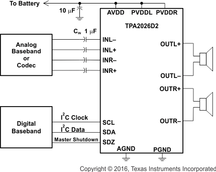
10.2.1 TPA2026D2 With Differential Input Signals
 Figure 49. Typical Application Schematic With Differential Input Signals
10.2.1.1 Design Requirements
For this design example, use the parameters listed in Table 13.
Table 13. Design Procedure
| PARAMETER | EXAMPLE VALUE |
|---|---|
| Power supply | 5 V |
| Enable inputs | High > 1.3 V |
| Low < 0.6 V | |
| Speaker | 8 Ω |
10.2.1.2 Detailed Design Procedure
10.2.1.2.1 Surface Mount Capacitor
Temperature and applied DC voltage influence the actual capacitance of high-K materials. Table 14 shows the relationship between the different types of high-K materials and their associated tolerances, temperature coefficients, and temperature ranges. Notice that a capacitor made with X5R material can lose up to 15% of its capacitance within its working temperature range.
In an application, the working capacitance of components made with high-K materials is generally much lower than nominal capacitance. A worst-case result with a typical X5R material might be –10% tolerance, –15% temperature effect, and –45% DC voltage effect at 50% of the rated voltage. This particular case would result in a working capacitance of 42% (0.9 × 0.85 × 0.55) of the nominal value.
Select high-K ceramic capacitors according to the following rules:
- Use capacitors made of materials with temperature coefficients of X5R, X7R, or better.
- Use capacitors with DC voltage ratings of at least twice the application voltage. Use minimum 10-V capacitors for the TPA2026D2.
- Choose a capacitance value at least twice the nominal value calculated for the application. Multiply the nominal value by a factor of 2 for safety. If a 10-μF capacitor is required, use 20 µF.
The preceding rules and recommendations apply to capacitors used in connection with the TPA2026D2. The TPA2026D2 cannot meet its performance specifications if the rules and recommendations are not followed.
Table 14. Typical Tolerance and Temperature Coefficient of Capacitance by Material
| MATERIAL | COG/NPO | X7R | X5R |
|---|---|---|---|
| Typical tolerance | ±5% | ±10% | 80/–20% |
| Temperature | ±30 ppm | ±15% | 22/–82% |
| Temperature range | –55 to 125°C | –55 to 125°C | –30 to 85°C |
10.2.1.2.2 Decoupling Capacitor, CS
The TPA2026D2 is a high-performance Class-D audio amplifier that requires adequate power supply decoupling to ensure the efficiency is high and total harmonic distortion (THD) is low. For higher frequency transients, spikes, or digital hash on the line, a good low equivalent-series-resistance (ESR) 1-μF ceramic capacitor (typically) placed as close as possible to the device PVDD (L, R) lead works best. Placing this decoupling capacitor close to the TPA2026D2 is important for the efficiency of the Class-D amplifier, because any resistance or inductance in the trace between the device and the capacitor can cause a loss in efficiency. For filtering lower-frequency noise signals, a 4.7 μF or greater capacitor placed near the audio power amplifier would also help, but it is not required in most applications because of the high PSRR of this device.
10.2.1.2.3 Input Capacitors, CI
The input capacitors and input resistors form a high-pass filter with the corner frequency, fC, determined in Equation 5.

The value of the input capacitor is important to consider as it directly affects the bass (low frequency) performance of the circuit. Speakers in wireless phones cannot usually respond well to low frequencies, so the corner frequency can be set to block low frequencies in this application. Not using input capacitors can increase output offset. Equation 6 is used to solve for the input coupling capacitance. If the corner frequency is within the audio band, the capacitors must have a tolerance of ±10% or better, because any mismatch in capacitance causes an impedance mismatch at the corner frequency and below.

10.2.1.3 Application Curves
For application curves, see the figures listed in Table 15.
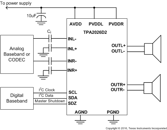
10.2.2 TPA2026D2 With Single-Ended Input Signal
 Figure 50. Typical Application Schematic With Single-Ended Input Signal
10.2.2.1 Design Requirements
For this design example, use the parameters listed in Table 13.
10.2.2.2 Detailed Design Procedure
For the design procedure see Detailed Design Procedure from the previous section
10.2.2.3 Application Curves
For application curves, see the figures listed in Table 15.