ZHCS760H February   2012  – June 2018 TLV62130 , TLV62130A

PRODUCTION DATA.  

  1. 特性
  2. 应用
  3. 说明
    1.     Device Images
      1.      典型应用原理图
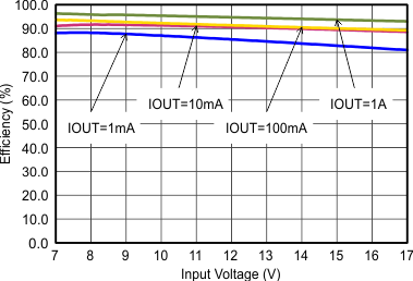
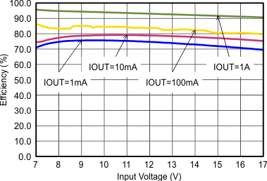
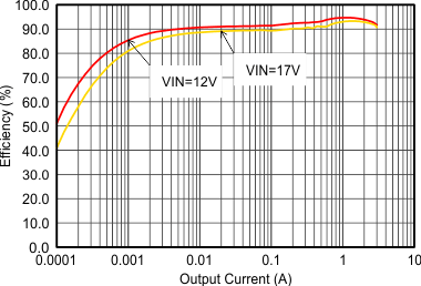
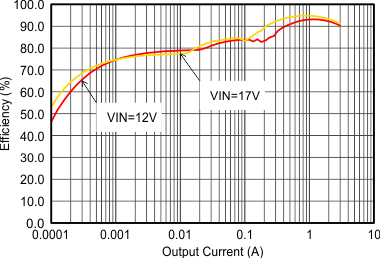
      2.      效率与输出电流间的关系
  4. 修订历史记录
  5. Device Comparison Table
  6. Pin Configuration and Functions
    1.     Pin Functions
  7. Specifications
    1. 7.1 Absolute Maximum Ratings
    2. 7.2 ESD Ratings
    3. 7.3 Recommended Operating Conditions
    4. 7.4 Thermal Information
    5. 7.5 Electrical Characteristics
    6. 7.6 Typical Characteristics
  8. Detailed Description
    1. 8.1 Overview
    2. 8.2 Functional Block Diagram
    3. 8.3 Feature Description
      1. 8.3.1 Enable / Shutdown (EN)
      2. 8.3.2 Soft Start / Tracking (SS/TR)
      3. 8.3.3 Power Good (PG)
      4. 8.3.4 Pin-Selectable Output Voltage (DEF)
      5. 8.3.5 Frequency Selection (FSW)
      6. 8.3.6 Undervoltage Lockout (UVLO)
      7. 8.3.7 Thermal Shutdown
    4. 8.4 Device Functional Modes
      1. 8.4.1 Pulse Width Modulation (PWM) Operation
      2. 8.4.2 Power Save Mode Operation
      3. 8.4.3 100% Duty-Cycle Operation
      4. 8.4.4 Current Limit and Short Circuit Protection
  9. Application and Implementation
    1. 9.1 Application Information
    2. 9.2 Typical Application
      1. 9.2.1 Design Requirements
      2. 9.2.2 Detailed Design Procedure
        1. 9.2.2.1 Custom Design With WEBENCH® Tools
        2. 9.2.2.2 Programming the Output Voltage
        3. 9.2.2.3 External Component Selection
          1. 9.2.2.3.1 Inductor Selection
          2. 9.2.2.3.2 Capacitor Selection
            1. 9.2.2.3.2.1 Output Capacitor
            2. 9.2.2.3.2.2 Input Capacitor
            3. 9.2.2.3.2.3 Soft Start Capacitor
        4. 9.2.2.4 Tracking Function
        5. 9.2.2.5 Output Filter and Loop Stability
      3. 9.2.3 Application Curves
    3. 9.3 System Examples
      1. 9.3.1 LED Power Supply
      2. 9.3.2 Active Output Discharge
      3. 9.3.3 Inverting Power Supply
      4. 9.3.4 Various Output Voltages
  10. 10Power Supply Recommendations
  11. 11Layout
    1. 11.1 Layout Guidelines
    2. 11.2 Layout Example
    3. 11.3 Thermal Considerations
  12. 12器件和文档支持
    1. 12.1 器件支持
      1. 12.1.1 第三方产品免责声明
      2. 12.1.2 开发支持
        1. 12.1.2.1 使用 WEBENCH® 工具创建定制设计
    2. 12.2 接收文档更新通知
    3. 12.3 文档支持
      1. 12.3.1 相关文档
    4. 12.4 相关链接
    5. 12.5 社区资源
    6. 12.6 商标
    7. 12.7 静电放电警告
    8. 12.8 术语表
  13. 13机械、封装和可订购信息

封装选项

机械数据 (封装 | 引脚)
散热焊盘机械数据 (封装 | 引脚)
订购信息

Application Curves

VIN = 12 V, VOUT = 3.3 V, TA = 25°C, (unless otherwise noted)
TLV62130 TLV62130A SLVSAG7_eff50iouthalf.gif
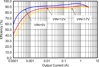
Figure 8. Efficiency With 1.25 MHz, Vout = 5 V
TLV62130 TLV62130A SLVSAG7_eff50ioutfull.gif
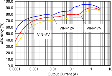
Figure 10. Efficiency With 2.5 MHz, Vout = 5 V
TLV62130 TLV62130A SLVSAG7_eff33iouthalf.gif
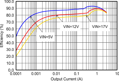
Figure 12. Efficiency With 1.25 MHz, Vout = 3.3 V
TLV62130 TLV62130A SLVSAG7_eff33ioutfull.gif
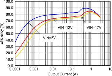
Figure 14. Efficiency With 2.5 MHz, Vout = 3.3 V
TLV62130 TLV62130A SLVSAG7_eff18iouthalf.gif
Figure 16. Efficiency With 1.25 MHz, Vout = 1.8 V
TLV62130 TLV62130A SLVSAG7_eff09iouthalf.gif
Figure 18. Efficiency With 1.25 MHz, Vout = 0.9 V
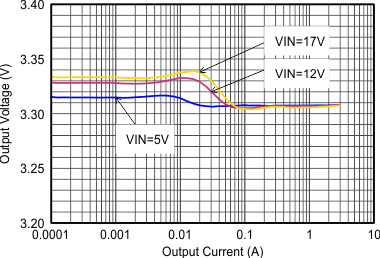
TLV62130 TLV62130A SLVSAG7_loadreg.gif
Figure 20. Output Voltage Accuracy (Load Regulation)
TLV62130 TLV62130A SLVSAG7_fswvin.gif
FSW=Low
Figure 22. Switching Frequency
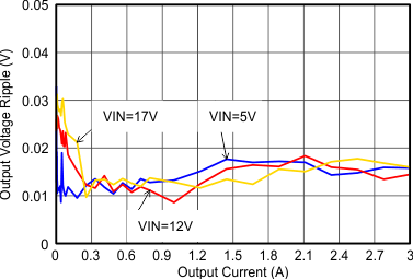
TLV62130 TLV62130A SLVSAG7_voutripple.gif
Figure 24. Output Voltage Ripple
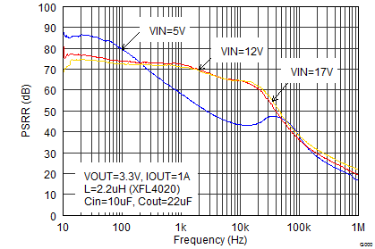
TLV62130 TLV62130A SLVSAG7_psrrhigh.png
Iout=1A
Figure 26. Power Supply Rejection Ratio, FSW = 2.5 MHz
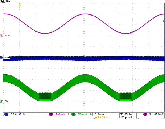
TLV62130 TLV62130A SLVSAG7_mode01.gifFigure 28. PWM-PSM-Transition
(VIN = 12 V, VOUT=3.3 V with 50 mV/Div)
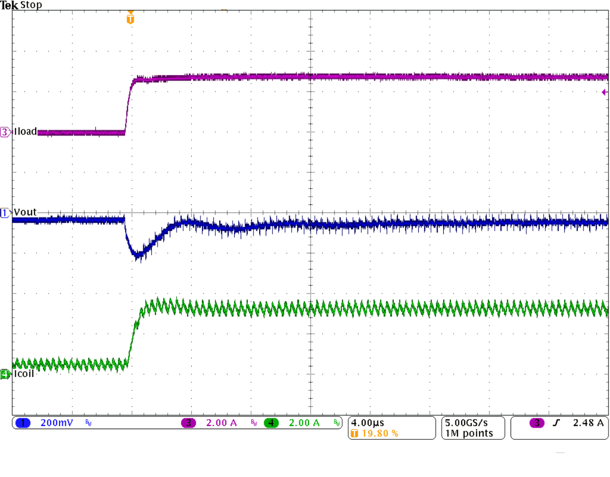
TLV62130 TLV62130A SLVSAG7_loadtranrise.gifFigure 30. Load Transient Response of Figure 29,
Rising Edge
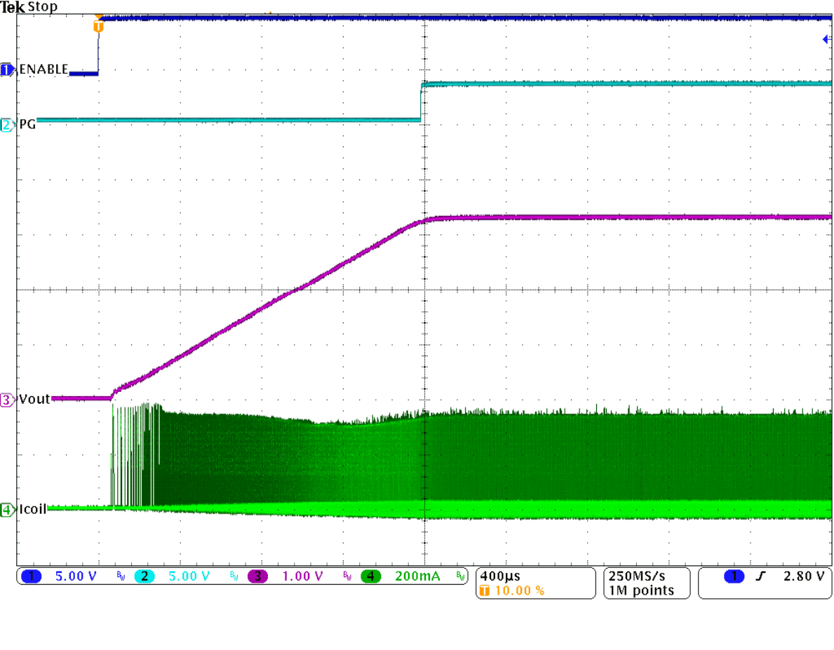
TLV62130 TLV62130A SLVSAG7_stuplow.gifFigure 32. Startup into 100 mA
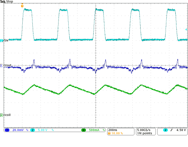
TLV62130 TLV62130A SLVSAG7_PWMtyp.gifFigure 34. Typical Operation in PWM Mode
(IOUT = 1 A)
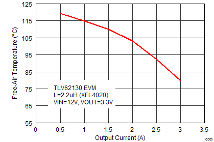
TLV62130 TLV62130A SLVSB74_ambienttmp.png
Figure 36. Maximum Ambient Temperature (FSW = 2.5 MHz)
TLV62130 TLV62130A SLVSAG7_eff50vinhalf.gif
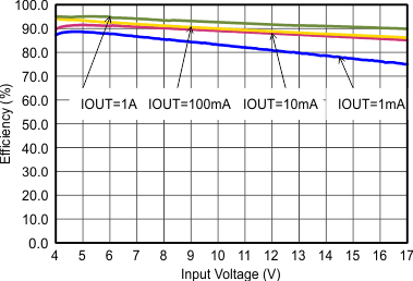
Figure 9. Efficiency With 1.25 MHz, Vout = 5 V
TLV62130 TLV62130A SLVSAG7_eff50vinfull.gif
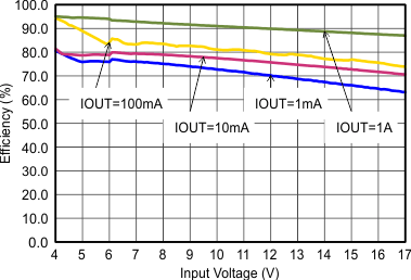
Figure 11. Efficiency With 2.5 MHz, Vout = 5 V
TLV62130 TLV62130A SLVSAG7_eff33vinhalf.gif
Figure 13. Efficiency With 1.25 MHz, Vout = 3.3 V
TLV62130 TLV62130A SLVSAG7_eff33vinfull.gif
Figure 15. Efficiency With 2.5 MHz, Vout = 3.3 V
TLV62130 TLV62130A SLVSB74_eff18vinhalf.png
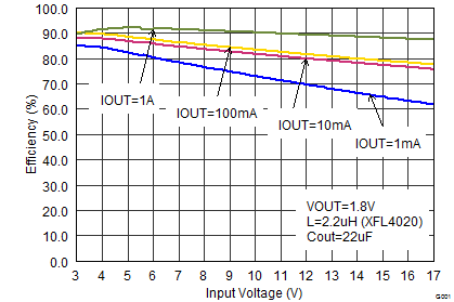
Figure 17. Efficiency With 1.25 MHz, Vout = 1.8 V
TLV62130 TLV62130A SLVSB74_eff09vinhalf.png
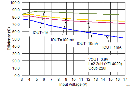
Figure 19. Efficiency With 1.25 MHz, Vout = 0.9 V
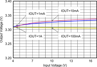
TLV62130 TLV62130A SLVSAG7_linereg.gif
Figure 21. Output Voltage Accuracy (Line Regulation)
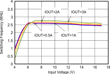
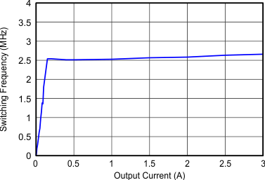
TLV62130 TLV62130A SLVSAG7_fswiout.gif
FSW=Low
Figure 23. Switching Frequency
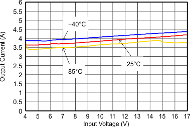
TLV62130 TLV62130A SLVSAG7_ioutmax.gif
Figure 25. Maximum Output Current
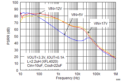
TLV62130 TLV62130A SLVSAG7_psrrlow.png
Iout=0.1A
Figure 27. Power Supply Rejection Ratio, FSW = 2.5 MHz
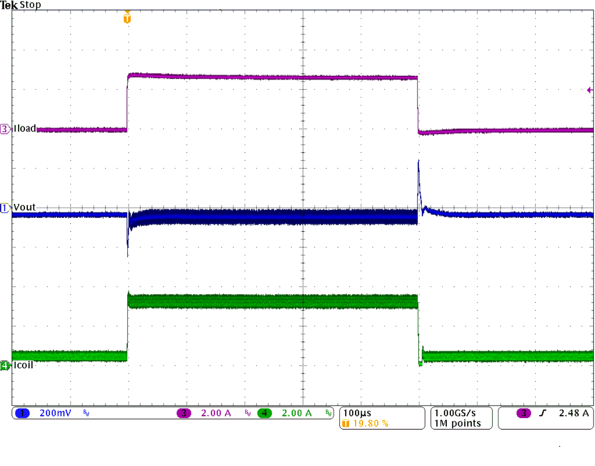
TLV62130 TLV62130A SLVSAG7_loadtranfull.gifFigure 29. Load Transient Response
(IOUT = 0.5 to 3 to 0.5 A)
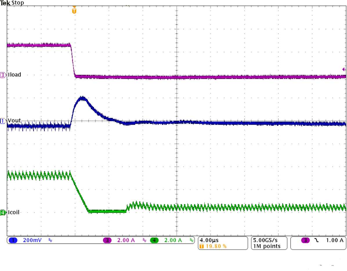
TLV62130 TLV62130A SLVSAG7_loadtranfall.gifFigure 31. Load Transient Response of Figure 29,
Falling Edge
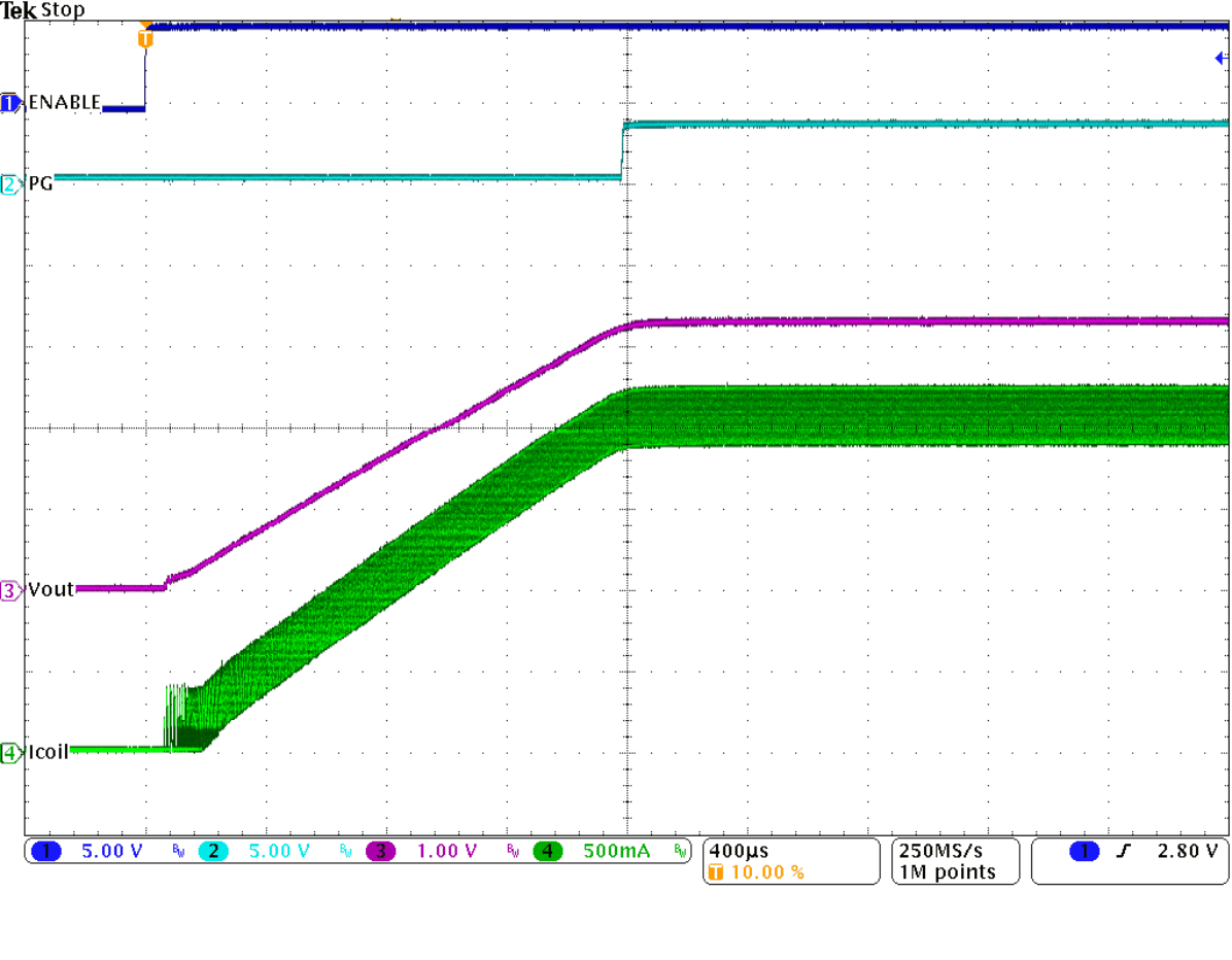
TLV62130 TLV62130A SLVSAG7_stuphigh.gifFigure 33. Startup into 3 A
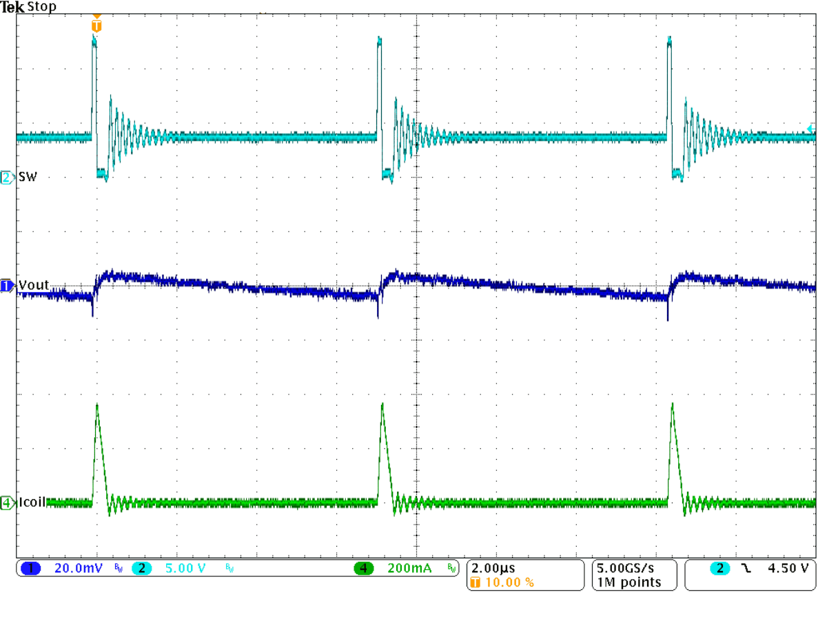
TLV62130 TLV62130A SLVSAG7_PSMtyp.gifFigure 35. Typical Operation in Power Save Mode
(IOUT = 10 mA)
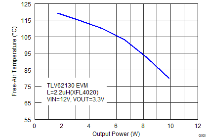
TLV62130 TLV62130A SLVSB74_powertmp.png
Figure 37. Maximum Ambient Temperature (FSW = 2.5 MHz)

sp