SLVSAF0A August 2010 – May 2015 TLV61225
PRODUCTION DATA.
8 Application and Implementation
NOTE
Information in the following applications sections is not part of the TI component specification, and TI does not warrant its accuracy or completeness. TI’s customers are responsible for determining suitability of components for their purposes. Customers should validate and test their design implementation to confirm system functionality.
8.1 Application Information
The TLV61225 is intended for systems which are powered by a single-cell battery to up to two Alkaline, NiCd, or NiMH cells with a typical terminal voltage from 0.7 V to 3.3 V and can output 3.3-V voltage. Additionally, any other voltage source with a typical output voltage from 0.7 V to 3.3 V can be used with the TLV61225.
8.2 Typical Application
 Figure 8. Typical Application Schematic
8.2.1 Design Requirements
In this example, TLV61225 is used to design a 3.3-V power supply with up to 15-mA output current capability. The TLV61225 can be powered by a single-cell battery to up to two Alkaline, NiCd or NiMH cells with a typical terminal voltage from 0.7 V to 3.5 V. In this example, the input voltage range is from 0.8 V to 1.5 V for single-cell Alkaline battery input design.
Table 2. List of Components
| COMPONENT REFERENCE | PART NUMBER | MANUFACTURER | VALUE | |
|---|---|---|---|---|
| C1 | GRM188R60J106ME84D | Murata | 10 μF, 6.3 V | |
| C2 | GRM188R60J106ME84D | Murata | 10 μF, 6.3 V | |
| L1 | EPL3015-472MLB | Coilcraft | 4.7 μH | |
8.2.2 Detailed Design Procedure
8.2.2.1 Programming the Output Voltage
At fixed voltage versions, the output voltage is programmed by an internal resistor divider. The FB pin is used to sense the output voltage. To configure the devices properly, the FB pin must be connected directly to VOUT.
8.2.2.2 Inductor Selection
To make sure that the TLV61225 devices can operate, a suitable inductor must be connected between pin VIN and pin L. Inductor values of 4.7 μH show good performance over the whole input and output voltage range.
Due to the fixed inductor current ripple control the switching frequency is defined by the inductor value. For a given switching frequency, input and output voltage the required inductance can be estimated using Equation 1.

Using inductor values greater than 4.7 μH can improve efficiency because higher values cause lower switching frequency and less switching losses. TI does not recommend using inductor values below 2.2 μH.
To ensure reliable operation of the TLV61225 under all load conditions, TI recommends using inductors with a current rating of 400 mA or higher. This will cover normal operation including current peaks during line and load transients.
Table 3 lists the inductor series from different suppliers have been used with the TLV61225 converter:
Table 3. List of Inductors
| VENDOR | INDUCTOR SERIES |
|---|---|
| Coilcraft | EPL3015 |
| EPL2010 | |
| Murata | LQH3NP |
| Tajo Yuden | NR3015 |
| Wurth Elektronik | WE-TPC Typ S |
8.2.2.3 Capacitor Selection
8.2.2.3.1 Input Capacitor
TI recommends using at least a 10-μF input capacitor to improve transient behavior of the regulator and EMI behavior of the total power supply circuit. TI also recommends placing a ceramic capacitor placed as close as possible to the VIN and GND pins of the IC.
8.2.2.3.2 Output Capacitor
For the output capacitor C2,TI recommends using small ceramic capacitors placed as close as possible to the VOUT and GND pins of the IC. There are no minimum output capacitor ESR requirements for maintaining control loop stability. If the application requires the use of large capacitors which cannot be placed close to the IC, TI recommends using a small ceramic capacitor with an capacitance value in the range of 2.2μF in parallel to the large capacitor. Place this small capacitor as close as possible to the VOUT and GND pins of the IC.
A minimum capacitance value of 4.7 μF should be used, TI recommends using 10 μF. To calculate the required output capacitance in case an inductor with a value higher than 4.7 μH has been selected Equation 2 can be used.

8.2.3 Application Curves
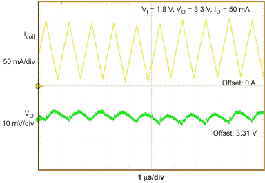
 Figure 9. Output Voltage Ripple
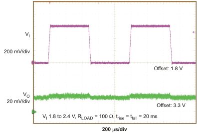
 Figure 11. Line Transient Response
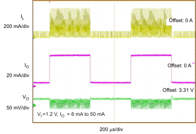
 Figure 10. Load Transient Response
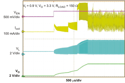
 Figure 12. Output Voltage vs Output Current and Input Voltage