ZHCSIW5C March 2019 – December 2021 TLV4021 , TLV4031 , TLV4041 , TLV4051
PRODUCTION DATA
- 1 特性
- 2 应用
- 3 说明
- 4 Revision History
- 5 Pin Configuration and Functions
- 6 Specifications
- 7 Typical Characteristics
- 8 Detailed Description
- 9 Application and Implementation
- 10Power Supply Recommendations
- 11Layout
- 12Device and Documentation Support
- 13Mechanical, Packaging, and Orderable Information
5 Pin Configuration and Functions
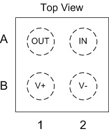
 Figure 5-1 YKA
Package
Figure 5-1 YKA
Package4-Bump DSBGA
Top View
Table 5-1 DSBGA Package Pin Functions
| PIN | I/O | DESCRIPTION | |
|---|---|---|---|
| NAME | NUMBER | ||
| OUT | A1 | O | Comparator output: OUT is push-pull on TLV4041/4051 and open-drain on TLV4021/4031 |
| V+ | B1 | P | Positive (highest) power supply |
| V– | B2 | P | Negative (lowest) power supply |
| IN | A2 | I | Comparator input: IN is non-Inverting on TLV4021/4041 and inverting on TLV4031/4051 |
Figure 5-2 SOT-23
Package
5-pin
Top View
5-pin
Top View
Table 5-2 SOT-23 Pin Functions
| PIN | I/O | DESCRIPTION | |
|---|---|---|---|
| NAME | NUMBER | ||
| V+ | 1 | P | Positive (highest) power supply |
| V- | 2 | P | Negative (lowest) power supply |
| NC | 3 | x | No connect; this pin is not internally connected to the die. It can be grounded if that is preferred in the system. |
| IN | 4 | I | Comparator input: IN is inverting on TLV4031/4051 |
| OUT | 5 | O | Comparator output: OUT is push-pull on TLV4041/4051 |