ZHCSF19 May   2016 TLV2369 , TLV369

PRODUCTION DATA.  

  1. 特性
  2. 应用
  3. 说明
  4. 修订历史记录
  5. Pin Configuration and Functions
  6. Specifications
    1. 6.1 Absolute Maximum Ratings
    2. 6.2 ESD Ratings
    3. 6.3 Recommended Operating Conditions
    4. 6.4 Thermal Information: TLV369
    5. 6.5 Thermal Information: TLV2369
    6. 6.6 Electrical Characteristics
    7. 6.7 Typical Characteristics
  7. Detailed Description
    1. 7.1 Overview
    2. 7.2 Functional Block Diagram
    3. 7.3 Feature Description
      1. 7.3.1 Operating Voltage
      2. 7.3.2 Input Common-Mode Voltage Range
      3. 7.3.3 Protecting Inputs from Overvoltage
    4. 7.4 Device Functional Modes
  8. Application and Implementation
    1. 8.1 Application Information
    2. 8.2 Typical Application
      1. 8.2.1 Design Requirements
      2. 8.2.2 Detailed Design Procedure
      3. 8.2.3 Application Curve
    3. 8.3 System Examples
      1. 8.3.1 Battery Monitoring
      2. 8.3.2 Window Comparator
  9. Power Supply Recommendations
  10. 10Layout
    1. 10.1 Layout Guidelines
    2. 10.2 Layout Example
  11. 11器件和文档支持
    1. 11.1 文档支持
      1. 11.1.1 相关文档
        1. 11.1.1.1 相关链接
    2. 11.2 社区资源
    3. 11.3 商标
    4. 11.4 静电放电警告
    5. 11.5 Glossary
  12. 12机械、封装和可订购信息

封装选项

机械数据 (封装 | 引脚)
散热焊盘机械数据 (封装 | 引脚)
订购信息

5 Pin Configuration and Functions

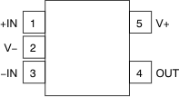
TLV369: DCK Package
5-Pin SC70
Top View
TLV369 TLV2369 po_sc70-5_bos414.gif

Pin Functions: TLV369

PIN I/O DESCRIPTION
NAME TLV369
DCK (SC70)
–IN 3 I Negative (inverting) input
+IN 1 I Positive (noninverting) input
OUT 4 O Output
V– 2 Negative (lowest) power supply or ground (for single-supply operation)
V+ 5 Positive (highest) power supply
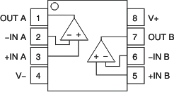
TLV2369: D Package
8-Pin SOIC
Top View
TLV369 TLV2369 po_so_msop_bos406.gif
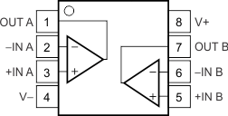
TLV2369: DGK Package
8-Pin VSSOP
Top View
TLV369 TLV2369 po_msop-8_bos757.gif

Pin Functions: TLV2369

PIN I/O DESCRIPTION
NAME TLV2369
D (SOIC) DGK (VSSOP)
–IN A 2 2 I Inverting input, channel A
–IN B 6 6 I Inverting input, channel B
+IN A 3 3 I Noninverting input, channel A
+IN B 5 5 I Noninverting input, channel B
OUT A 1 1 O Output, channel A
OUT B 7 7 O Output, channel B
V– 4 4 Negative (lowest) power supply
V+ 8 8 Positive (highest) power supply