ZHCSF22 May 2016 TLC6C5912
PRODUCTION DATA.
9 Application and Implementation
NOTE
Information in the following applications sections is not part of the TI component specification, and TI does not warrant its accuracy or completeness. TI’s customers are responsible for determining suitability of components for their purposes. Customers should validate and test their design implementation to confirm system functionality.
9.1 Application Information
The TLC6C5912 device is a serial-in, parallel-out, power logic 8-bit shift register with low-side open-drain DMOS output rating of 40 V and 50-mA continuous sink-current capabilities when VCC= 5 V. The device is designed to drive resistive loads and is particularly well-suited as an interface between a microcontroller and LEDs or lamps. The device also provides up to 2000 V of ESD protection when tested using the human body model and 200 V when using the machine model.
9.2 Typical Application
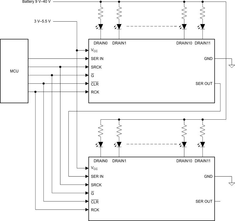
Figure 13 shows a typical cascade application circuit with two TLC6C5912 chips configured to cascade topology. The MCU generates all the input signals.
 Figure 13. Typical Application Circuit
9.2.1 Design Requirements
Table 1 lists the parameters for this design example.
Table 1. Design Parameters
| DESIGN PARAMETER | EXAMPLE VALUE |
|---|---|
| Vbattery | 9 V to 40 V |
| VCC _ 1 | 3.3 V |
| I(D0), I(D1), I(D2), I(D3) , I(D4), I(D5), I(D6), I(D7), I(D8), I(D9), I(D10), I(D11) | 30 mA |
| VCC _ 2 | 5 V |
| I(D12), I(D13), I(D14), I(D15) , I(D16), I(D17), I(D18), I(D19), I(D20), I(D21), I(D122), I(D23) | 50 mA |
9.2.2 Detailed Design Procedure
To begin the design process, the designer must decide on a few parameters:
- Vsupply: LED supply voltage
- VDx: LED forward voltage
- I: LED current
After determining the parameters, calculate the resistor in series with LED using Equation 1.
9.2.3 Application Curve
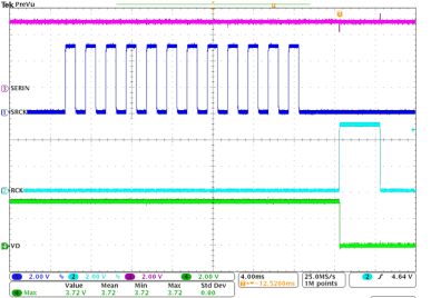
 Figure 14. TLC6C5912 Application Waveform