ZHCSEM2A August 2015 – August 2015 TLC6C5712-Q1
PRODUCTION DATA.
- 1 特性
- 2 应用范围
- 3 说明
- 4 修订历史记录
- 5 Pin Configuration and Functions
- 6 Specifications
-
7 Detailed Description
- 7.1 Overview
- 7.2 Functional Block Diagram
- 7.3
Feature Description
- 7.3.1 Power-On Reset (POR)
- 7.3.2 Error Feedback
- 7.3.3 PWM Input
- 7.3.4 Constant-Current Output
- 7.3.5 Advanced Diagnostics
- 7.3.6 Register Protection
- 7.3.7 Serial Interface - SPI
- 7.3.8 Thermal Information
- 7.4 Device Functional Modes
- 7.5
Register Maps
- 7.5.1 WRITE_MAP0 Register (address = 40h) [reset = 00h]
- 7.5.2 WRITE_MAP1 Register (address = 41h) [reset = 00h]
- 7.5.3 WRITE_MAP2 Register (address = 42h) [reset = 00h]
- 7.5.4 WRITE_MAP3 Register (address = 43h) [reset = 00h]
- 7.5.5 WRITE_MAP4 Register (address = 44h) [reset = 00h]
- 7.5.6 WRITE_MAP5 Register (address = 45h) [reset = 00h]
- 7.5.7 WRITE_CORR0 Register (address = 46h) [reset = 00h]
- 7.5.8 WRITE_CORR1 Register (address = 47h) [reset = 00h]
- 7.5.9 WRITE_CORR2 Register (address = 48h) [reset = 00h]
- 7.5.10 WRITE_CORR3 Register (address = 49h) [reset = 00h]
- 7.5.11 WRITE_CORR4 Register (address = 4Ah) [reset = 00h]
- 7.5.12 WRITE_CORR5 Register (address = 4Bh) [reset = 00h]
- 7.5.13 WRITE_CORR6 Register (address = 4Ch) [reset = 00h]
- 7.5.14 WRITE_CORR7 Register (address = 4Dh) [reset = 00h]
- 7.5.15 WRITE_CORR8 Register (address = 4Eh) [reset = 00h]
- 7.5.16 WRITE_CORR9 Register (address = 4Fh) [reset = 00h]
- 7.5.17 WRITE_CORR10 Register (address = 50h) [reset = 00h]
- 7.5.18 WRITE_CORR11 Register (address = 51h) [reset = 00h]
- 7.5.19 WRITE_CH_ON_MASK0 Register (address = 52h) [reset = 3Fh]
- 7.5.20 WRITE_CH_ON_MASK1 Register (address = 53h) [reset = 3Fh]
- 7.5.21 WRITE_SHORT_MASK0 Register (address = 54h) [reset = 3Fh]
- 7.5.22 WRITE_SHORT_MASK1 Register (address = 55h) [reset = 3Fh]
- 7.5.23 WRITE_SHORT_GND_MASK0 Register (address = 56h) [reset = 3Fh]
- 7.5.24 WRITE_SHORT_GND_MASK1 Register (address = 57h) [reset = 3Fh]
- 7.5.25 WRITE_OPEN_MASK0 Register (address = 58h) [reset = 3Fh]
- 7.5.26 WRITE_OPEN_MASK1 Register (address = 59h) [reset = 3Fh]
- 7.5.27 WRITE_PWM_FAULT_MASK Register (address = 60h) [reset = 3Fh]
- 7.5.28 RESET_POR Register (address = 61h) [reset = 00h]
- 7.5.29 RESET_STATUS Register (address = 62h) [reset = 00h]
- 7.5.30 SOFTWARE_POR Register (address = 63h) [reset = 00h]
- 7.5.31 WRITE_DIS_PULL_UP_0 Register (address = 64h) [reset = 00h]
- 7.5.32 WRITE_DIS_PULL_UP_1 Register (address = 65h) [reset = 00h]
- 7.5.33 WRITE_ERROR_MASK Register (address = 66h) [reset = 00h]
- 7.5.34 WRITE_MISC_CMD Register (address = 67h) [reset = 00h]
- 7.5.35 LOCK_MAP Register (address = 68h) [reset = 00h]
- 7.5.36 LOCK_CORR Register (address = 69h) [reset = 00h]
- 7.5.37 LOCK_MASK Register (address = 6Ah) [reset = 00h]
- 7.5.38 LOCK_MISC Register (address = 6Bh) [reset = 00h]
- 7.5.39 UNLOCK_MAP Register (address = 6Ch) [reset = 00h]
- 7.5.40 UNLOCK_CORR Register (address = 6Dh) [reset = 00h]
- 7.5.41 UNLOCK_MASK Register (address = 6Eh) [reset = 00h]
- 7.5.42 UNLOCK_MISC Register (address = 6Fh) [reset = 00h]
- 7.5.43 READ_MAP0 Register (address = 80h) [reset = 00h]
- 7.5.44 READ_MAP1 Register (address = 81h) [reset = 00h]
- 7.5.45 READ_MAP2 Register (address = 82h) [reset = 00h]
- 7.5.46 READ_MAP3 Register (address = 83h) [reset = 00h]
- 7.5.47 READ_MAP4 Register (address = 84h) [reset = 00h]
- 7.5.48 READ_MAP5 Register (address = 85h) [reset = 00h]
- 7.5.49 READ_CORR0 Register (address = 86h) [reset = 00h]
- 7.5.50 READ_CORR1 Register (address = 87h) [reset = 00h]
- 7.5.51 READ_CORR2 Register (address = 88h) [reset = 00h]
- 7.5.52 READ_CORR3 Register (address = 89h) [reset = 00h]
- 7.5.53 READ_CORR4 Register (address = 8Ah) [reset = 00h]
- 7.5.54 READ_CORR5 Register (address = 8Bh) [reset = 00h]
- 7.5.55 READ_CORR6 Register (address = 8Ch) [reset = 00h]
- 7.5.56 READ_CORR7 Register (address = 8Dh) [reset = 00h]
- 7.5.57 READ_CORR8 Register (address = 8Eh) [reset = 00h]
- 7.5.58 READ_CORR9 Register (address = 8Fh) [reset = 00h]
- 7.5.59 READ_CORR10 Register (address = 90h) [reset = 00h]
- 7.5.60 READ_CORR11 Register (address = 91h) [reset = 00h]
- 7.5.61 READ_CH_ON_MASK0 Register (address = 92h) [reset = 3Fh]
- 7.5.62 READ_CH_ON_MASK1 Register (address = 93h) [reset = 3Fh]
- 7.5.63 READ_SHORT_MASK0 Register (address = 94h) [reset = 3Fh]
- 7.5.64 READ_SHORT_MASK1 Register (address = 95h) [reset = 3Fh]
- 7.5.65 READ_SHORT_GND_MASK0 Register (address = 96h) [reset = 3Fh]
- 7.5.66 READ_SHORT_GND_MASK1 Register (address = 97h) [reset = 3Fh]
- 7.5.67 READ_OPEN_MASK0 Register (address = 98h) [reset = 3Fh]
- 7.5.68 READ_OPEN_MASK1 Register (address = 99h) [reset = 3Fh]
- 7.5.69 READ_SHORT_FAULT0 (address = 9Ah) [reset = 00h]
- 7.5.70 READ_SHORT_FAULT1 (address = 9Bh) [reset = 00h]
- 7.5.71 READ_SHORT_GND_FAULT0 (address = 9Ch) [reset = 00h]
- 7.5.72 READ_SHORT_GND_FAULT1 (address = 9Dh) [reset = 00h]
- 7.5.73 READ_OPEN_FAULT0 (address = 9Eh) [reset = 00h]
- 7.5.74 READ_OPEN_FAULT1 (address = 9Fh) [reset = 00h]
- 7.5.75 READ_PWM_FAULT_MASK Register (address = A1h) [reset = 3Fh]
- 7.5.76 READ_STATUS0 (address = A2h) [reset = 40h]
- 7.5.77 READ_STATUS1 (address = A3h) [reset = 00h]
- 7.5.78 READ_DIS_PULL_UP_0 Register (address = A4h) [reset = 00h]
- 7.5.79 READ_DIS_PULL_UP_1 Register (address = A5h) [reset = 00h]
- 7.5.80 READ_ERROR_MASK (address = A6h) [reset = 00h]
- 7.5.81 READ_MISC_CMD Register (address = A7h) [reset = 00h]
- 7.5.82 READ_ADSHORT0 (address = A8h) [reset = 00h]
- 7.5.83 READ_ADSHORT1 (address = A9h) [reset = 00h]
- 8 Application and Implementation
- 9 Power Supply Recommendations
- 10Layout
- 11器件和文档支持
- 12机械、封装和可订购信息
8 Application and Implementation
NOTE
Information in the following applications sections is not part of the TI component specification, and TI does not warrant its accuracy or completeness. TI’s customers are responsible for determining suitability of components for their purposes. Customers should validate and test their design implementation to confirm system functionality.
8.1 Application Information
The TLC6C5712-Q1 device is capable of driving different numbers of LEDs with accurate current driving and the most-advanced diagnostics. The device is suitable for automotive cluster tell-tale lighting, gear-shifter PRNDL indicators, and other safety-critical LED applications.
8.2 Typical Applications
8.2.1 Multiple Devices Connected in Cascade
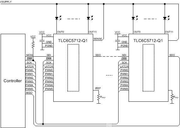
The TLC6C5712-Q1 design supports multiple devices in cascaded daisy-chain mode. Each communication sequence must only have one LATCH rising edge and, therefore, cannot be split into multiple smaller sequences.
 Figure 106. Application Schematic for TLC6C5712-Q1 Devices Connected in Cascade
8.2.1.1 Design Requirements
For this design example, use the parameters listed in Table 55.
8.2.1.2 Detailed Design Procedure
This design has multiple TLC6C5712-Q1 devices connected by a SPI daisy chain. Use Equation 5 to calculate the reference resistor value.

Use Equation 6 to calculate the dot correction for each channel.

8.2.1.3 Application Curves
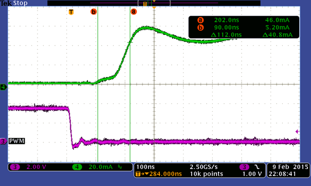
 Figure 107. PWM Delay and Output Rise Time
CH3: PWM0, CH4: OUT0
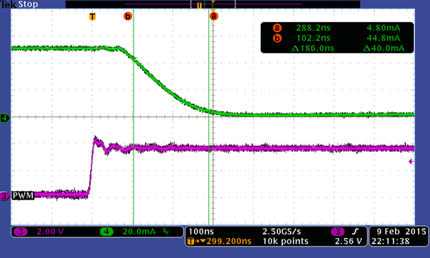
 Figure 108. PWM Delay and Output Fall Time
CH3: PWM0, CH4: OUT0
8.2.2 Parallel Channels for Driving Higher Current
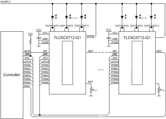
In some applications, capability to drive higher current is needed. To deliver higher current while maintaining adjacent-short detection capability, channels with odd numbers can be shorted together; similarly, channels with even numbers can be shorted together. If odd and even numbers are shorted together, the device reports a false error during adjacent-pin short detection.
 Figure 109. Application Schematic for TLC6C5712-Q1 Devices With Parallel Outputs
8.2.2.1 Design Requirements
For this design example, use the parameters listed in Table 56.
8.2.2.2 Detailed Design Procedure
This design has multiple TLC6C5712-Q1 devices connected by a SPI daisy chain. Use Equation 7 to calculate the reference resistor value.

Use Equation 8 to calculate the dot correction for each channel.
