SCLS715A March 2009 – November 2015 TLC59208F
PRODUCTION DATA.
- 1 Features
- 2 Applications
- 3 Description
- 4 Revision History
- 5 Description (continued)
- 6 Pin Configuration and Functions
- 7 Specifications
- 8 Parameter Measurement Information
-
9 Detailed Description
- 9.1 Overview
- 9.2 Functional Block Diagram
- 9.3 Feature Description
- 9.4 Device Functional Modes
- 9.5 Programming
- 9.6
Register Maps
- 9.6.1
Register Descriptions
- 9.6.1.1 Mode Register 1 (MODE1)
- 9.6.1.2 Mode Register 2 (MODE2)
- 9.6.1.3 Individual Brightness Control Registers (PWM0-PWM7)
- 9.6.1.4 Group Duty Cycle Control Register (GRPPWM)
- 9.6.1.5 Group Frequency Register (GRPFREQ)
- 9.6.1.6 LED Driver Output State Registers (LEDOUT0, LEDOUT1)
- 9.6.1.7 I2C Bus Sub-Address Registers 1 to 3 (SUBADR1-SUBADR3)
- 9.6.1.8 LED All Call I2C Bus Address Register (ALLCALLADR)
- 9.6.1
Register Descriptions
- 10Application and Implementation
- 11Power Supply Recommendations
- 12Layout
- 13Device and Documentation Support
- 14Mechanical, Packaging, and Orderable Information
封装选项
机械数据 (封装 | 引脚)
散热焊盘机械数据 (封装 | 引脚)
- RGY|16
订购信息
1 Features
- Eight LED Drivers (Each Output Programmable at OFF, ON, Programmable LED Brightness, Programmable Group Dimming/Blinking Mixed With Individual LED Brightness)
- Eight Open-Drain Output Channels
- 256-Step (8-Bit) Linear Programmable Brightness Per LED Output Varying From Fully Off (Default) to Maximum Brightness Using a 97-kHz PWM Signal
- 256-Step Group Brightness Control Allows General Dimming [Using a 190-Hz PWM Signal From Fully Off to Maximum Brightness (Default)]
- 256-Step Group Blinking With Frequency Programmable From 24 Hz to 10.73 s and Duty Cycle From 0% to 99.6%
- 64 Programmable Slave Addresses Using Three Hardware Address Pins
- Four Software Programmable I2C Bus Addresses (One LED Group Call Address and Three LED Sub Call Addresses) Allow Groups of Devices to be Simultaneously Addressed Any Combination (For Example, One Register Used for ‘All Call’ so That All the TLC59208Fs on the I2C Bus Can be Simultaneously Addressed and the Second Register Used for Three Different Addresses so That One Third of All Devices on the Bus Can be Simultaneously Addressed)
- Software Enable and Disable for I2C Bus Address
- Software Reset Feature (SWRST Call) Allows the Device to be Reset Through the I2C Bus
- Up to 14 Possible Hardware Adjustable Individual I2C Bus Addresses Per Device so That Each Device Can be Programmed
- Up to 64 Possible Hardware Adjustable Individual I2C Bus Addresses Per Device so That Each Device Can be Programmed Individually
- Output State Change Programmable on the Acknowledge or the STOP Command to Update Outputs Byte-by-Byte or All at the Same Time (Default to Change on STOP)
- Maximum Output Current: 50 mA
- Maximum Output Voltage: 17 V
- 25-MHz Internal Oscillator Requires no External Components
- 1-MHz Fast-Mode Plus (FM+) Compatible I2C Bus Interface With 30-mA High Drive Capability on SDA Output for Driving High Capacitive Buses
- Internal Power-On Reset
- Noise Filter on SCL/SDA Inputs
- No Glitch on Power Up
- Active-Low Reset (RESET)
- Supports Hot Insertion
- Low Standby Current
- 3.3-V or 5-V Supply Voltage
- 5.5-V Tolerant Inputs
- Packages Offered: 16-Pin Thin Shrink Small-Outline Package [TSSOP (PW)], 16-Pin Quad Flatpack No Lead [QFN (RGY)]
- –40°C to 85°C Operation
2 Applications
- Gaming
- Small Signage
- Industrial Equipment
3 Description
The TLC59208F is an I2C bus controlled 8-bit LED driver optimized for red/green/blue/amber (RGBA) color mixing applications. Each LED output has its own 8-bit resolution (256 steps) fixed frequency individual PWM controller that operates at 97 kHz with a duty cycle that is adjustable from 0% to 99.6% to allow the LED to be set to a specific brightness value.
Device Information(1)
| PART NUMBER | PACKAGE | BODY SIZE (NOM) |
|---|---|---|
| TLC59208F | TSSOP (16) | 5.00 mm × 4.40 mm |
| VQFN (16) | 4.00 mm × 3.50 mm |
- For all available packages, see the orderable addendum at the end of the data sheet.
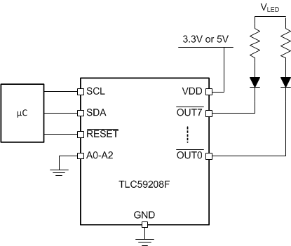
Application Schematic
