SLVS529D April 2004 – January 2015 TL1431-EP
PRODUCTION DATA.
- 1 Features
- 2 Applications
- 3 Description
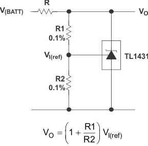
- 4 Simplified Schematic
- 5 Revision History
- 6 Pin Configuration and Functions
- 7 Specifications
- 8 Parameter Measurement Information
- 9 Detailed Description
- 10Application and Implementation
- 11Power Supply Recommendations
- 12Layout
- 13Device and Documentation Support
- 14Mechanical, Packaging, and Orderable Information
10 Application and Implementation
NOTE
Information in the following applications sections is not part of the TI component specification, and TI does not warrant its accuracy or completeness. TI’s customers are responsible for determining suitability of components for their purposes. Customers should validate and test their design implementation to confirm system functionality.
10.1 Application Information
The ability to set the shunt voltage, VKA, to any voltage between VREF and the maximum rated voltage for the shunt regulator provides a lot of flexibility. It takes two resistors to set the shunt voltage. In an ideal common anode shunt regulator, the shunt voltage would be VREF × (R1/R2 + 1).
Real world shunt regulators have limited gain, non-zero reference input current, and suffer from cathode voltage modulation. This application report derives comprehensive formulas that accurately represent the relationship between the shunt voltage and feedback resistors. It also shows a practical example.
Shunt Regulator Limitations
Real world shunt regulators have three parameters that should be considered.
- Dynamic impedance, ZKA
- Reference pin current, IREF
- Ratio of change in reference voltage to the change in cathode voltage, ΔVREF/ΔVKA.
The first parameter will cause a VREF shift for all VKA values and the last two only apply when VKA, is set greater than VREF.
ZKA offsets the VREF in direct proportion to the cathode current. The data sheet generally specifies VREF at a specific current. At any other current ZKA impacts VREF.
IREF causes an inequality in the feedback resistor currents which changes the effective DC feedback ratio. This factor is often included in data sheet formulas.
ΔVREF/ΔVKA specifies how much the VREF voltage changes when the cathode voltage changes. This is a frequently ignored factor although the effect can be significant.
10.2 Typical Application
10.2.1 Design Requirements
To calculate the values for resistors R1 and R2, the values of the following parameters must be known: the feedback current, (IFB), cathode current, (IKA), and desired shunt voltage, (VKA).
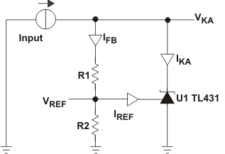
The Electrical Characteristics table specifies when VKA = VREF and IKA is 10 mA the nominal VREF, (labeled VNOM) is 2.5 V. The reference voltage varies with cathode voltage at two different rates. The reference voltage is –1.1 mV/V from VREF to 10 V then –1.5 mV/V above 10 V. The reference pin current is 4 µA.
The ZKA parameter offsets VREF by (IKA – INOM) × ZKA .
In addition, the ΔVREF / ΔVKA parameter offsets VREF by either –1.1 mV × (VKA – 2.5 V) if VKA ≤ 10 V or –8.25 mV –1.5 mV/V × (VKA – 10 V) if VKA>10 V. The –8.25-mV constant is the VREF offset as VKA changes from
VNOM to 10 V, (10 V – 2.5 V) × –1.1 mV/V.
Therefore:
If VKA ≤ 10 V then;
If VKA > 10 then;
Now that the value of VREF is calculated, use Equation 1 and Equation 2 to calculate the value of R1 and R2.
NOTE
R2 has less current than R1.
10.2.2 Detailed Design Procedure
The goal of the design is: the TL1431 cathode set to 12 V, the cathode current at 2 mA, and a feedback current of 0.2 mA.
Using the formula derived in the general example for VKA>10 V.
Using Equation 5 and Equation 6, the value of VREF = 2.473 V
Using Equation 7 and Equation 8, the value of R1 = 46.285 kΩ
Using Equation 9 and Equation 10, the value of R2 = 12.617 kΩ
The closest standard 1% resistor values are R1 = 46.4 kΩ and R2 = 12.7 kΩ. Other resistor combinations may provide a shunt voltage that is centered better. A formula to test for R1 values that may be closer to standard values using standard R2 resistors is R1= (VKA – VREF) / (VREF / R2 + IREF).
10.2.3 Application Curves
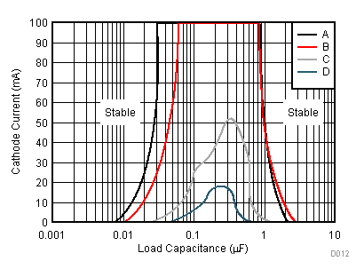 Figure 22. Stability Bounderies for load capacitance on Shunt Regulator
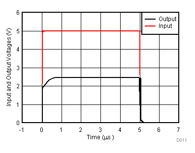 Figure 23. Pulse Response at Startup of Shunt Regulator