ZHCSI92D May   2018  – November 2020 TAS5805M

PRODUCTION DATA  

  1. 特性
  2. 应用
  3. 说明
  4. Revision History
  5. Device Comparison Table
  6. Pin Configuration and Functions
  7. Specifications
    1. 6.1 Absolute Maximum Ratings
    2. 6.2 ESD Ratings
    3. 6.3 Recommended Operating Conditions
    4. 6.4 Thermal Information
    5. 6.5 Electrical Characteristics
    6. 6.6 Timing Requirements
    7. 6.7 Typical Characteristics
      1. 6.7.1 Bridge Tied Load (BTL) Configuration Curves with 1SPW Mode
      2. 6.7.2 Bridge Tied Load (BTL) Configuration Curves with BD Mode
      3. 6.7.3 Bridge Tied Load (BTL) Configuration Curves with Ferrite Bead + Capacitor as the Output Filter
      4. 6.7.4 Parallel Bridge Tied Load (PBTL) Configuration with 1SPW Modulation
      5. 6.7.5 Parallel Bridge Tied Load (PBTL) Configuration with BD Modulation
  8. Parameter Measurement Information
  9. Detailed Description
    1. 7.1 Overview
    2. 7.2 Functional Block Diagram
    3. 7.3 Feature Description
      1. 7.3.1 Power Supplies
      2. 7.3.2 Device Clocking
      3. 7.3.3 Serial Audio Port – Clock Rates
      4. 7.3.4 Clock Halt Auto-recovery
      5. 7.3.5 Sample Rate on the Fly Change
      6. 7.3.6 Serial Audio Port - Data Formats and Bit Depths
      7. 7.3.7 Digital Audio Processing
      8. 7.3.8 Class D Audio Amplifier
        1. 7.3.8.1 Speaker Amplifier Gain Select
        2. 7.3.8.2 Class D Loop Bandwidth and Switching Frequency Setting
    4. 7.4 Device Functional Modes
      1. 7.4.1 Software Control
      2. 7.4.2 Speaker Amplifier Operating Modes
        1. 7.4.2.1 BTL Mode
        2. 7.4.2.2 PBTL Mode
      3. 7.4.3 Low EMI Modes
        1. 7.4.3.1 Spread Spectrum
        2. 7.4.3.2 Channel to Channel Phase Shift
        3. 7.4.3.3 Multi-Devices PWM Phase Synchronization
      4. 7.4.4 Thermal Foldback
      5. 7.4.5 Device State Control
      6. 7.4.6 Device Modulation
        1. 7.4.6.1 BD Modulation
        2. 7.4.6.2 1SPW Modulation
        3. 7.4.6.3 Hybrid Modulation
    5. 7.5 Programming and Control
      1. 7.5.1 I2 C Serial Communication Bus
      2. 7.5.2 Slave Address
        1. 7.5.2.1 Random Write
        2. 7.5.2.2 Sequential Write
        3. 7.5.2.3 Random Read
        4. 7.5.2.4 Sequential Read
        5. 7.5.2.5 DSP Memory Book, Page and BQ Coefficients Update
        6. 7.5.2.6 Example Use
        7. 7.5.2.7 Checksum
          1. 7.5.2.7.1 Cyclic Redundancy Check (CRC) Checksum
          2. 7.5.2.7.2 Exclusive or (XOR) Checksum
      3. 7.5.3 Control via Software
        1. 7.5.3.1 Startup Procedures
        2. 7.5.3.2 Shutdown Procedures
        3. 7.5.3.3 Protection and Monitoring
          1. 7.5.3.3.1 Overcurrent Shutdown (OCSD)
          2. 7.5.3.3.2 Speaker DC Protection
          3. 7.5.3.3.3 Device Over Temperature Protection
          4. 7.5.3.3.4 Device Over Voltage/Under Voltage Protection
            1. 7.5.3.3.4.1 Over Voltage Protection
            2. 7.5.3.3.4.2 Under Voltage Protection
          5. 7.5.3.3.5 Clock Fault
    6. 7.6 Register Maps
      1. 7.6.1 CONTROL PORT Registers
  10. Application and Implementation
    1. 8.1 Application Information
      1. 8.1.1 Bootstrap Capacitors
      2. 8.1.2 Inductor Selections
      3. 8.1.3 Power Supply Decoupling
      4. 8.1.4 Output EMI Filtering
    2. 8.2 Typical Applications
      1. 8.2.1 2.0 (Stereo BTL) System
        1. 8.2.1.1 Design Requirements
        2. 8.2.1.2 Detailed Design Procedures
          1. 8.2.1.2.1 Step 1: Hardware Integration
          2. 8.2.1.2.2 Step 2: Speaker Tuning
          3. 8.2.1.2.3 Step 3: Software Integration
        3. 8.2.1.3 Application Curves
          1. 8.2.1.3.1 Audio Performance
          2. 8.2.1.3.2 EN55022 Conducted Emissions Results with Ferrite Bead as output filter
          3. 8.2.1.3.3 EN55022 Radiated Emissions Results with Ferrite Bead as output filter
      2. 8.2.2 MONO (PBTL) Systems
        1. 8.2.2.1 Design Requirements
        2. 8.2.2.2 Detailed Design Procedure
        3. 8.2.2.3 Application Curves
      3. 8.2.3 Advanced 2.1 System (Two TAS5805M Devices)
  11. Power Supply Recommendations
    1. 9.1 DVDD Supply
    2. 9.2 PVDD Supply
  12. Layout
    1. 9.1 Layout Guidelines
      1. 9.1.1 General Guidelines for Audio Amplifiers
      2. 9.1.2 Importance of PVDD Bypass Capacitor Placement on PVDD Network
      3. 9.1.3 Optimizing Thermal Performance
        1. 9.1.3.1 Device, Copper, and Component Layout
        2. 9.1.3.2 Stencil Pattern
          1. 9.1.3.2.1 PCB footprint and Via Arrangement
          2. 9.1.3.2.2 Solder Stencil
    2. 9.2 Layout Example
  13. 10Device and Documentation Support
    1. 10.1 Device Support
      1. 10.1.1 Device Nomenclature
      2. 10.1.2 Development Support
    2. 10.2 Receiving Notification of Documentation Updates
    3. 10.3 支持资源
    4. 10.4 Trademarks
    5. 10.5 静电放电警告
    6. 10.6 术语表
  14. 11Mechanical, Packaging, and Orderable Information

封装选项

请参考 PDF 数据表获取器件具体的封装图。

机械数据 (封装 | 引脚)
  • PWP|28
散热焊盘机械数据 (封装 | 引脚)
订购信息

Bridge Tied Load (BTL) Configuration Curves with 1SPW Mode

Free-air room temperature 25°C (unless otherwise noted.) Measurements were made using TAS5805MEVM board and Audio Precision System 2722 with Analog Analyzer filter set to 20-kHz brickwall filter. All measurements taken with audio frequency set to 1 kHz and device PWM Modulation mode set to 1SPW mode with Class D Bandwidth = 120 kHz for 576 kHz Fsw and Class D Bandwidth = 175 kHz for 768 kHz Fsw (Listed in Register 0x53) unless otherwise noted.
GUID-C6B61576-021C-4699-A008-D4FBE61F5400-low.gif
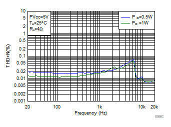
PVDD = 5 V 4.7µH+0.68µF
FSW = 576 kHz 1SPW Modulation Load = 4Ω
Figure 6-1 THD+N vs Frequency-BTL
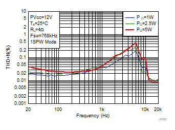
GUID-97E8C0C6-F3BC-423E-82D7-B5962877966A-low.gif
PVDD = 12 V 10µH+0.68µF
FSW = 768 kHz 1SPW Modulation Load = 4Ω
Figure 6-3 THD+N vs Frequency-BTL
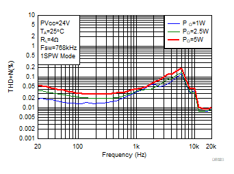
GUID-FF5B24F9-6FA5-448E-AD49-45B42C900478-low.gif
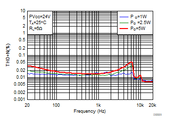
PVDD = 24 V 10µH+0.68µF
FSW = 768 kHz 1SPW Modulation Load = 4Ω
Figure 6-5 THD+N vs Frequency-BTL
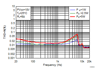
GUID-10BCD44D-74DD-4085-A8E1-EDF2A8E07C18-low.gif
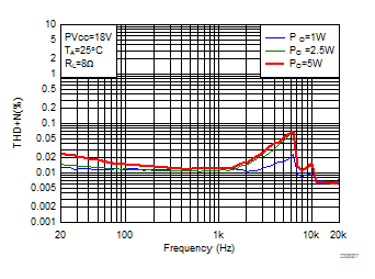
PVDD = 18 V 10µH+0.68µF
FSW = 768 kHz 1SPW Modulation Load = 6Ω
Figure 6-7 THD+N vs Frequency-BTL
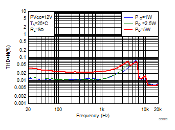
GUID-0198CB21-4E77-4720-90FE-140696F9FA37-low.gif
PVDD = 12 V 4.7uH+0.68uF
FSW = 768 kHz 1SPW Modulation Load = 8Ω
Figure 6-9 THD+N vs Frequency-BTL
GUID-51FF66E3-4FD6-42D7-881A-0E114DE48537-low.gif
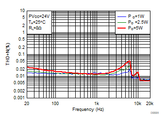
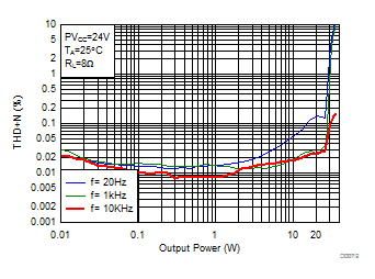
PVDD = 24 V 10µH+0.68µF
FSW = 768 kHz 1SPW Modulation Load = 8Ω
Figure 6-11 THD+N vs Frequency-BTL
GUID-A35AC2FA-A1F1-449F-BC5E-0DCD0A3FD9B9-low.gif
NOTE: Dashed lines represent thermally limited region for the continuous output power.
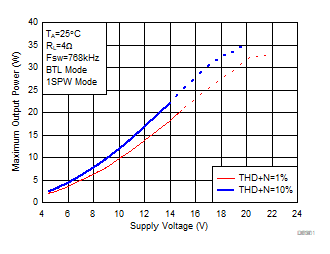
PVDD = 4.5 V~24V 10µH+0.68µF
FSW = 768 kHz 1SPW Modulation Load = 4Ω
Figure 6-13 Output Power vs Supply Voltage-BTL
GUID-77A29471-C14B-4CFD-8A88-624845C6EEFF-low.gif
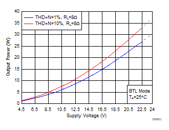
PVDD = 4.5 V~24V 10µH+0.68µF
FSW = 768 kHz 1SPW Modulation Load = 8Ω
Figure 6-15 Output Power vs Supply Voltage-BTL
GUID-0344A79A-44E3-4ECA-BA58-35C300BA7C08-low.gif
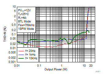
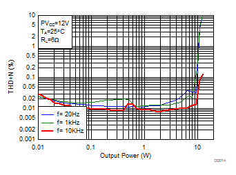
PVDD = 12V 10µH+0.68µF
FSW = 768 kHz 1SPW Modulation Load = 4Ω
Figure 6-17 THD+N vs Output Power-BTL
GUID-987E50E0-FE3D-4AB0-B256-12C879AB3F1D-low.gif
PVDD = 12V 4.7µH+0.68µF
FSW = 768 kHz 1SPW Modulation Load = 6Ω
Figure 6-19 THD+N vs Output Power-BTL
GUID-E8CAF405-4B94-4D89-A02C-6793439A87CC-low.gif
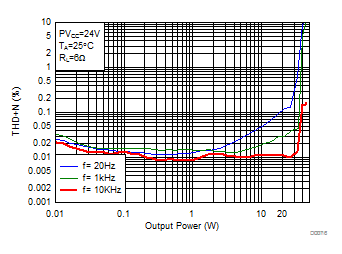
PVDD = 24V 10µH+0.68µF
FSW = 768 kHz 1SPW Modulation Load = 6Ω
Figure 6-21 THD+N vs Output Power-BTL
GUID-4B147A7C-934F-443A-8FA9-47D7A4441CFF-low.gif
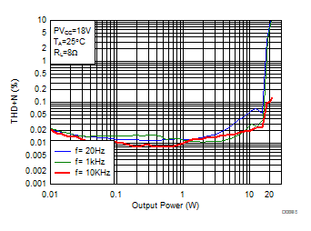
PVDD = 18V 10µH+0.68µF
FSW = 768 kHz 1SPW Modulation Load = 8Ω
Figure 6-23 THD+N vs Output Power-BTL
GUID-9C06DF86-3A2D-4C1E-89AF-CE23E3A97141-low.gif
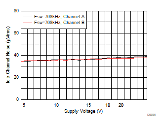
PVDD = 4.5V~24V 10µH+0.68µF
FSW = 768 kHz 1SPW Modulation Load = 8Ω
Figure 6-25 Idle Channel Noise vs PVDD-BTL
GUID-FB8293B8-61BE-4513-B0BC-DE13471C7C30-low.gif
PVDD = 18V 10µH+0.68µF Pout=1W
FSW = 768 kHz 1SPW Modulation Load = 6Ω
Figure 6-27 Crosstalk
GUID-6CF6704A-7174-4BB0-BD7B-851733B94AFE-low.gif
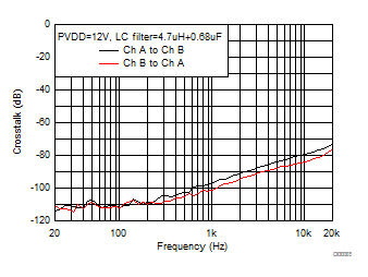
PVDD = 12V 4.7µH+0.68µF Pout=1W
FSW = 768 kHz 1SPW Modulation Load = 8Ω
Figure 6-29 Crosstalk
GUID-4EBD6719-4205-45F4-8E4E-5E82F00C5AB8-low.gif
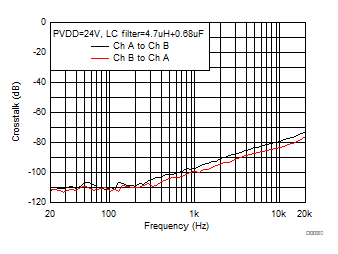
PVDD = 24V 10µH+0.68µF Pout=1W
FSW = 768 kHz 1SPW Modulation Load = 8Ω
Figure 6-31 Crosstalk
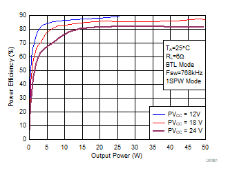
GUID-2B6198B5-CCF1-47EF-982D-333C93851A86-low.gif
PVDD = 12V/18V/24V 10µH+0.68µF
FSW = 768 kHz 1SPW Modulation Load = 6Ω
Figure 6-33 Efficiency vs Output Power-BTL
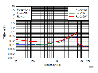
GUID-2AC4E24E-3DD0-4FCB-8B3D-51CE6B7B0895-low.gif
PVDD = 7.4 V 4.7µH+0.68µF
FSW = 576 kHz 1SPW Modulation Load = 4Ω
Figure 6-2 THD+N vs Frequency-BTL
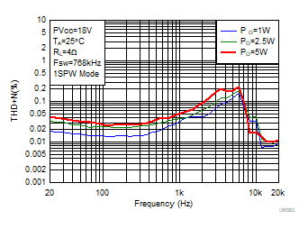
GUID-A43C43A6-6053-4525-B2BC-8E191C4CEC9F-low.gif
PVDD = 18 V 10µH+0.68µF
FSW = 768 kHz 1SPW Modulation Load = 4Ω
Figure 6-4 THD+N vs Frequency-BTL
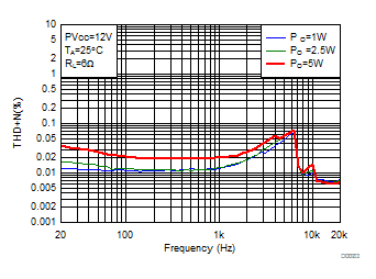
GUID-03EACF79-1D91-49CE-8D78-78B3457646B5-low.gif
PVDD = 12 V 4.7µH+0.68µF
FSW = 768 kHz 1SPW Modulation Load = 6Ω
Figure 6-6 THD+N vs Frequency-BTL
GUID-78AA886E-90B4-4BDD-843D-A90E117F736B-low.gif
PVDD = 24 V 10µH+0.68µF
FSW = 768 kHz 1SPW Modulation Load = 6Ω
Figure 6-8 THD+N vs Frequency-BTL
GUID-16907CF6-1AFD-43D5-B0C0-3D1CFDA69376-low.gif
PVDD = 18 V 10µH+0.68µF
FSW = 768 kHz 1SPW Modulation Load = 8Ω
Figure 6-10 THD+N vs Frequency-BTL
GUID-04C79853-32B3-449E-B6F3-CC562EA5F853-low.gif
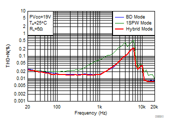
PVDD = 19 V 10µH+0.68µF POUT = 5W
FSW = 384 kHz BD/1SPW/Hybrid Load = 6Ω
Figure 6-12 THD+N vs Frequency-BTL
GUID-48D6B649-A415-4D05-B45E-AC214C971E3B-low.gif
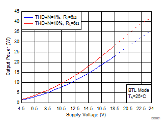
NOTE: Dashed lines represent thermally limited region for the continuous output power.
PVDD = 4.5 V~24V 10µH+0.68µF
FSW = 768 kHz 1SPW Modulation Load = 6Ω
Figure 6-14 Output Power vs Supply Voltage-BTL
GUID-497B3035-004B-4AA6-AD01-CE76F6B957D5-low.gif
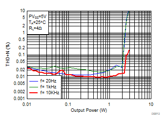
PVDD = 5V 4.7µH+0.68µF
FSW = 768 kHz 1SPW Modulation Load = 4Ω
Figure 6-16 THD+N vs Output Power-BTL
GUID-63F1AF3F-DE24-4658-B99C-3E2E136961E3-low.gif
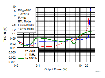
PVDD = 18V 10µH+0.68µF
FSW = 768 kHz 1SPW Modulation Load = 4Ω
Figure 6-18 THD+N vs Output Power-BTL
GUID-2369CE40-8CFE-453D-8EE2-D2AF26A58873-low.gif
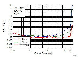
PVDD = 18V 10µH+0.68µF
FSW = 768 kHz 1SPW Modulation Load = 6Ω
Figure 6-20 THD+N vs Output Power-BTL
GUID-E5FC3DB4-185B-4FCF-9CD2-1BF3F88428DC-low.gif
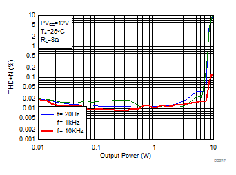
PVDD = 12V 4.7µH+0.68µF
FSW = 768 kHz 1SPW Modulation Load = 8Ω
Figure 6-22 THD+N vs Output Power-BTL
GUID-18BE29AC-718B-4051-B32C-191AC3D83FB8-low.gif
PVDD = 24V 10µH+0.68µF
FSW = 768 kHz 1SPW Modulation Load = 8Ω
Figure 6-24 THD+N vs Output Power-BTL
GUID-A9E07CCD-A298-4095-8929-81409FC717D6-low.gif
PVDD = 12V 4.7µH+0.68µF Pout=1W
FSW = 768 kHz 1SPW Modulation Load = 6Ω
Figure 6-26 Crosstalk
GUID-A9D03F58-24DE-4C76-98FF-979019F3E54C-low.gif
PVDD = 24V 10µH+0.68µF Pout=1W
FSW = 768 kHz 1SPW Modulation Load = 6Ω
Figure 6-28 Crosstalk
GUID-3102E945-A6B2-4EB8-AEA5-47768B70CB7F-low.gif
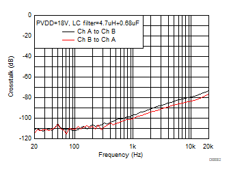
PVDD = 18V 10µH+0.68µF Pout=1W
FSW = 768 kHz 1SPW Modulation Load = 8Ω
Figure 6-30 Crosstalk
GUID-0FD29FD4-D403-4A30-BA7B-AFCDCEF1760D-low.gif
PVDD = 12V/18V/24V 10µH+0.68µF
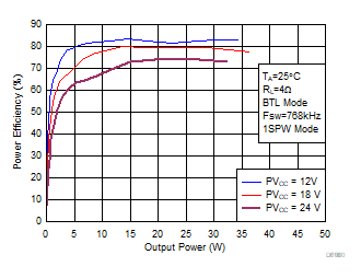
FSW = 768 kHz 1SPW Modulation Load = 4Ω
Figure 6-32 Efficiency vs Output Power-BTL
GUID-E292FEA4-0298-4B0A-AE77-4B7EF63A24A9-low.gif
PVDD = 12V/18V/24V 10µH+0.68µF
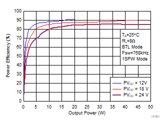
FSW = 768 kHz 1SPW Modulation Load = 8Ω
Figure 6-34 Efficiency vs Output Power-BTL