SLAS988B June 2014 – August 2015 TAS5756M
PRODUCTION DATA.
- 1 Features
- 2 Applications
- 3 Description
- 4 Revision History
- 5 Device Comparison Table
- 6 Pin Configuration and Functions
-
7 Specifications
- 7.1 Absolute Maximum Ratings
- 7.2 ESD Ratings
- 7.3 Recommended Operating Conditions
- 7.4 Thermal Information
- 7.5 Electrical Characteristics
- 7.6 MCLK Timing
- 7.7 Serial Audio Port Timing - Slave Mode
- 7.8 Serial Audio Port Timing - Master Mode
- 7.9 I2C Bus Timing - Standard
- 7.10 I2C Bus Timing - Fast
- 7.11 SPK_MUTE Timing
- 7.12 Power Dissipation
- 7.13 Typical Characteristics
-
8 Detailed Description
- 8.1 Overview
- 8.2 Functional Block Diagram
- 8.3
Feature Description
- 8.3.1 Power-on-Reset (POR) Function
- 8.3.2 Device Clocking
- 8.3.3
Serial Audio Port
- 8.3.3.1 Clock Master Mode from Audio Rate Master Clock
- 8.3.3.2 Clock Master from a Non-Audio Rate Master Clock
- 8.3.3.3 Clock Slave Mode with 4-Wire Operation (SCLK, MCLK, LRCK/FS, SDIN)
- 8.3.3.4 Clock Slave Mode with SLCK PLL to Generate Internal Clocks (3-Wire PCM)
- 8.3.3.5 Serial Audio Port - Data Formats and Bit Depths
- 8.3.3.6 Input Signal Sensing (Power-Save Mode)
- 8.3.3.7 Serial Data Output
- 8.3.4 Modulation Scheme
- 8.3.5 miniDSP Audio Processing Engine
- 8.3.6 Adjustable Amplifier Gain and Switching Frequency Selection
- 8.3.7
Error Handling and Protection Suite
- 8.3.7.1 Device Overtemperature Protection
- 8.3.7.2 SPK_OUTxx Overcurrent Protection
- 8.3.7.3 DC Offset Protection
- 8.3.7.4 Internal VAVDD Undervoltage-Error Protection
- 8.3.7.5 Internal VPVDD Undervoltage-Error Protection
- 8.3.7.6 Internal VPVDD Overvoltage-Error Protection
- 8.3.7.7 External Undervoltage-Error Protection
- 8.3.7.8 Internal Clock Error Notification (CLKE)
- 8.3.8 GPIO Port and Hardware Control Pins
- 8.3.9 I2C Communication Port
- 8.4 Device Functional Modes
-
9 Application and Implementation
- 9.1 Application Information
- 9.2
Typical Applications
- 9.2.1 2.0 (Stereo BTL) System
- 9.2.2 Mono (PBTL) Systems
- 9.2.3 2.1 (Stereo BTL + External Mono Amplifier) Systems
- 9.2.4 2.2 (Dual Stereo BTL) Systems
- 9.2.5 1.1 (Dual BTL, Bi-Amped) Systems
- 10Power Supply Recommendations
- 11Layout
- 12Device and Documentation Support
- 13Mechanical, Packaging, and Orderable Information
6 Pin Configuration and Functions
DCA Package
48-Pin HTSSOP With PowerPAD™
Top View
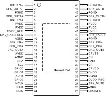
Pin Functions
| PIN | TYPE(1) | INTERNAL TERMINATION | DESCRIPTION | |
|---|---|---|---|---|
| NAME | NO. | |||
| ADR0 | 26 | DI | Figure 11 | Sets the LSB of the I2C address to 0 if pulled to GND, to 1 if pulled to DVDD |
| ADR1 | 20 | DI | Sets the second LSB of the I2C address to 0 if pulled to GND, to 1 if pulled to DVDD | |
| AGND | 10 | G | — | Ground reference for analog circuitry(2) |
| 15 | ||||
| AVDD | 14 | P | Figure 2 | Power supply for internal analog circuitry |
| BSTRPA– | 1 | P | Figure 3 | Connection point for the SPK_OUTA– bootstrap capacitor which is used to create a power supply for the high-side gate drive for SPK_OUTA– |
| BSTRPA+ | 5 | P | Connection point for the SPK_OUTA+ bootstrap capacitor which is used to create a power supply for the high-side gate drive for SPK_OUTA | |
| BSTRPB– | 48 | P | Connection point for the SPK_OUTB– bootstrap capacitor which is used to create a power supply for the high-side gate drive for SPK_OUTB– | |
| BSTRPB+ | 44 | P | Connection point for the SPK_OUTB+ bootstrap capacitor which is used to create a power supply for the high-side gate drive for SPK_OUTB+ | |
| CN | 34 | P | Figure 15 | Negative pin for capacitor connection used in the line--driver charge pump |
| CP | 32 | P | Figure 14 | Positive pin for capacitor connection used in the line-driver charge pump |
| CPVDD | 31 | P | Figure 2 | Power supply for charge pump circuitry |
| CPVSS | 35 | P | Figure 15 | –3.3-V supply generated by charge pump for the DAC |
| DAC_OUTA | 13 | AO | Figure 8 | Single-ended output for Channel A of the DAC |
| DAC_OUTB | 36 | AO | Single-ended output for Channel B of the DAC | |
| DGND | 29 | G | — | Ground reference for digital circuitry. Connect this pin to the system ground. |
| DVDD | 30 | P | Figure 2 | Power supply for the internal digital circuitry |
| DVDD_REG | 28 | P | Figure 16 | Voltage regulator derived from DVDD supply for use for internal digital circuitry. This pin is provided as a connection point for filtering capacitors for this supply and must not be used to power any external circuitry. |
| GND | 33 | G | — | Ground pin for device. This pin should be connected to the system ground. |
| GPIO0 | 18 | DI/O | Figure 11 | General purpose input/output pins (GPIOx) which can be incorporated in a HybridFlow for a given purpose. Refer to documentation of target HybridFlow to determine if any of these pins are required by the HybridFlow and, if so, how they are to be used. In most HybridFlows, presentation of a serial audio signal, called SDOUT, is done through GPIO2. |
| GPIO1 | 19 | |||
| GPIO2 | 21 | |||
| GVDD_REG | 8 | P | Figure 5 | Voltage regulator derived from PVDD supply to generate the voltage required for the gate drive of output MOSFETs. This pin is provided as a connection point for filtering capacitors for this supply and must not be used to power any external circuitry. |
| LRCK/FS | 25 | DI/O | Figure 12 | Word select clock for the digital signal that is active on the serial port's input data line. In I2S, LJ, and RJ, this corresponds to the left channel and right channel boundary. In TDM mode, this corresponds to the frame sync boundary. |
| MCLK | 22 | DI | Master clock used for internal clock tree and sub-circuit and state machine clocking | |
| PGND | 3 | G | — | Ground reference for power device circuitry. Connect this pin to the system ground. |
| 39 | ||||
| 46 | ||||
| PVDD | 6 | P | Figure 1 | Power supply for internal power circuitry |
| 7 | ||||
| 41 | ||||
| 42 | ||||
| 43 | ||||
| SCL | 17 | DI | Figure 10 | I2C serial control port clock |
| SCLK | 23 | DI/O | Figure 12 | Bit clock for the digital signal that is active on the input data line of the serial data port |
| SDA | 16 | DI/O | Figure 9 | I2C serial control port data |
| SDIN | 24 | D1 | Figure 12 | Data line to the serial data port |
| SPK_INA– | 11 | AI | Figure 7 | Negative pin for differential speaker amplifier input A |
| SPK_INA+ | 12 | AI | Positive pin for differential speaker amplifier input A | |
| SPK_INB– | 38 | AI | Negative pin for differential speaker amplifier input B | |
| SPK_INB+ | 37 | AI | Positive pin for differential speaker amplifier input B | |
| SPK_FAULT | 40 | DO | Figure 17 | Fault pin which is pulled low when an overcurrent, overtemperature, overvoltage, undervoltage, or DC detect event occurs |
| SPK_GAIN/FREQ | 9 | AI | Figure 6 | Sets the gain and switching frequency of the speaker amplifier, latched in upon start-up of the device. |
| SPK_OUTA– | 2 | AO | Figure 4 | Negative pin for differential speaker amplifier output A |
| SPK_OUTA+ | 4 | AO | Positive pin for differential speaker amplifier output A | |
| SPK_OUTB– | 47 | AO | Negative pin for differential speaker amplifier output B | |
| SPK_OUTB+ | 45 | AO | Positive pin for differential speaker amplifier output B | |
| SPK_MUTE | 27 | I | Figure 13 | Speaker amplifier mute which must be pulled low (connected to DGND) to mute the device and pulled high (connected to DVDD) to unmute the device. |
| Themal pad | G | — | Provides both electrical and thermal connection from the device to the board. A matching ground pad must be provided on the PCB and the device connected to it through solder. For proper electrical operation, this ground pad must be connected to the system ground. | |
(1) AI = Analog input, AO = Analog output, DI = Digital Input, DO = Digital Output, DI/O = Digital Bi-directional (input and output), P = Power, G = Ground (0 V)
(2) This pin should be connected to the system ground.
6.1 Internal Pin Configurations
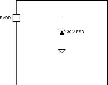 Figure 1. PVDD Pins
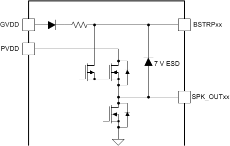 Figure 3. BSTRPxx Pins
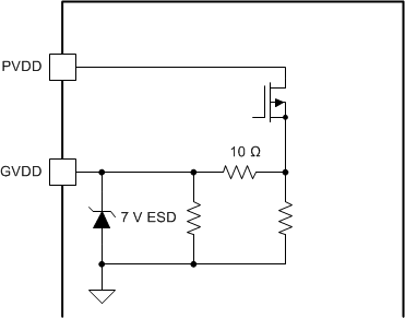 Figure 5. GVDD_REG Pin
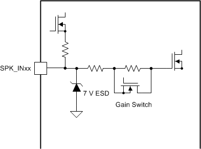 Figure 7. SPK_INxx Pins
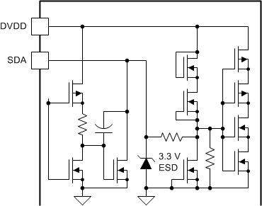 Figure 9. SDA Pin
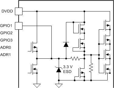 Figure 11. GPIO and ADR Pins
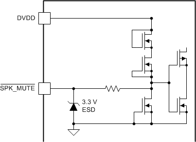 Figure 13. SPK_MUTE Pin
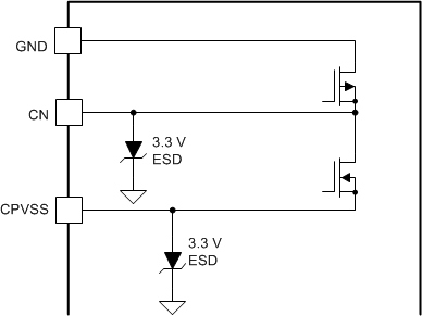 Figure 15. CN and CPVSS Pins
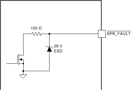 Figure 17. SPK_FAULT Pin
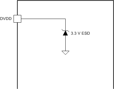 Figure 2. AVDD, DVDD and CPVDD Pins
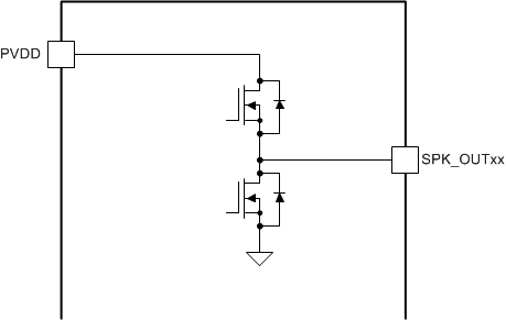 Figure 4. SPK_OUTxx Pins
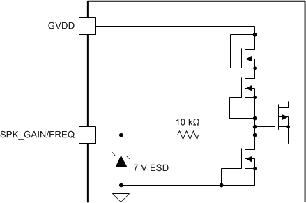 Figure 6. SPK_GAIN/FREQ Pin
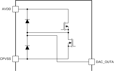 Figure 8. DAC_OUTx Pins
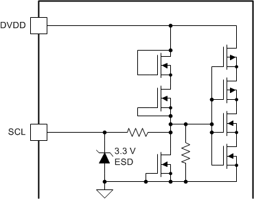 Figure 10. SCL Pin
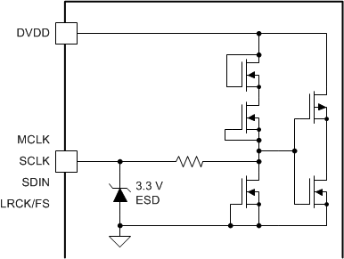 Figure 12. SCLK, BCLK, SDIN, and LRCK/FS Pins
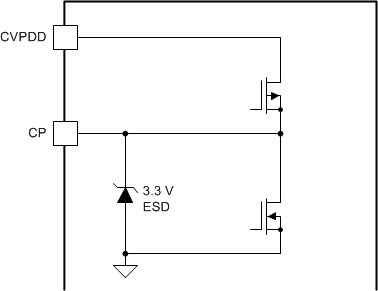 Figure 14. CP Pin
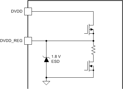 Figure 16. DVDD_REG Pin