SLLS259J November   1996  – October 2016 SN75LVDS82

PRODUCTION DATA.  

  1. Features
  2. Applications
  3. Description
  4. Revision History
  5. Description (continued)
  6. Pin Configuration and Functions
  7. Specifications
    1. 7.1 Absolute Maximum Ratings
    2. 7.2 ESD Ratings
    3. 7.3 Recommended Operating Conditions
    4. 7.4 Thermal Information
    5. 7.5 Electrical Characteristics
    6. 7.6 Timing Requirements
    7. 7.7 Switching Characteristics
    8. 7.8 Typical Characteristics 
  8. Parameter Measurement Information
    1. 8.1 Equivalent Input and Output Schematic Diagrams
  9. Detailed Description
    1. 9.1 Overview
    2. 9.2 Functional Block Diagram
    3. 9.3 Feature Description
      1. 9.3.1 LVDS Input Data
    4. 9.4 Device Functional Modes
      1. 9.4.1 Low Power Mode
      2. 9.4.2 Test Patterns
  10. 10Application and Implementation
    1. 10.1 Application Information
    2. 10.2 Typical Applications
      1. 10.2.1 Signal Connectivity
        1. 10.2.1.1 Design Requirements
        2. 10.2.1.2 Detailed Design Procedure
          1. 10.2.1.2.1 Power Up Sequence
        3. 10.2.1.3 Application Curves
  11. 11Power Supply Recommendations
    1. 11.1 Decoupling Capacitor Recommendations
  12. 12Layout
    1. 12.1 Layout Guidelines
    2. 12.2 Layout Example
  13. 13Device and Documentation Support
    1. 13.1 Receiving Notification of Documentation Updates
    2. 13.2 Community Resources
    3. 13.3 Trademarks
    4. 13.4 Electrostatic Discharge Caution
    5. 13.5 Glossary
  14. 14Mechanical, Packaging, and Orderable Information

封装选项

机械数据 (封装 | 引脚)
散热焊盘机械数据 (封装 | 引脚)
订购信息

Parameter Measurement Information

Equivalent Input and Output Schematic Diagrams

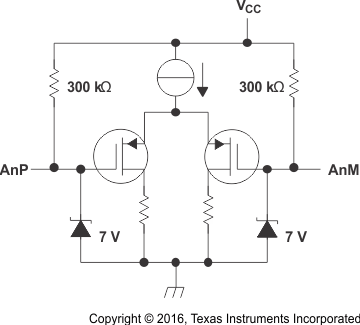
SN75LVDS82 sch_diag_lls259_3.gif Figure 8. LVDS Input
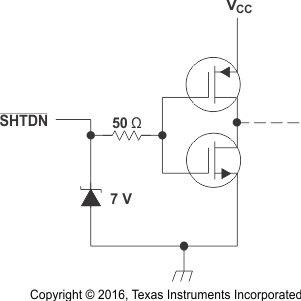
SN75LVDS82 sch_diag_lls259_1.gif Figure 9. SHTDN Input
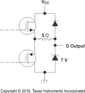
SN75LVDS82 sch_diag_lls259_2.gif Figure 10. Output
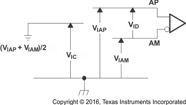
SN75LVDS82 pm_vdef_lls259.gif Figure 11. Voltage Definitions