SLRS007C November 1986 – January 2015 SN754410
PRODUCTION DATA.
- 1 Features
- 2 Applications
- 3 Description
- 4 Simplified Schematic
- 5 Revision History
- 6 Pin Configuration and Functions
- 7 Specifications
- 8 Parameter Measurement Information
- 9 Detailed Description
- 10Application and Implementation
- 11Power Supply Recommendations
- 12Layout
- 13Device and Documentation Support
- 14Mechanical, Packaging, and Orderable Information
7 Specifications
7.1 Absolute Maximum Ratings
over operating free-air temperature range (unless otherwise noted)(1)(2)| MIN | MAX | UNIT | ||
|---|---|---|---|---|
| VCC1 | Output supply voltage range | –0.5 | 36 | V |
| VCC2 | Output supply voltage range | –0.5 | 36 | V |
| VI | Input voltage | –0.5 | 36 | V |
| VO | Output voltage range | –3 | VCC2 + 3 | V |
| IP | Peak output current | ±2 | A | |
| IO | Continuous output current | ±1 | A | |
| PD | Continuous total power dissipation at (or below) 25°C free-air temperature(3) | 2075 | mW | |
| TA | Operating free-air temperature range | –40 | 85 | °C |
| TJ | Operating virtual junction temperature range | –40 | 150 | °C |
| Tstg | Storage temperature range | 260 | °C | |
(1) Stresses beyond those listed under Absolute Maximum Ratings may cause permanent damage to the device. These are stress ratings only, which do not imply functional operation of the device at these or any other conditions beyond those indicated under Recommended Operating Conditions. Exposure to absolute-maximum-rated conditions for extended periods may affect device reliability.
(2) All voltage values are with respect to network GND.
(3) For operation above 25°C free-air temperature, derate linearly at the rate of 16.6 mW/°C. To avoid exceeding the design maximum virtual junction temperature, these ratings should not be exceeded. Due to variations in individual device electrical characteristics and thermal resistance, the built-in thermal overload protection can be activated at power levels slightly above or below the rated dissipation.
7.2 Recommended Operating Conditions
over operating free-air temperature range (unless otherwise noted)| MIN | MAX | UNIT | |||
|---|---|---|---|---|---|
| VCC1 | Logic supply voltage | 4.5 | 5.5 | V | |
| VCC2 | Output supply voltage | 4.5 | 36 | V | |
| VIH | High-level input voltage | 2 | 5.5 | V | |
| VIL | Low-level input voltage | –0.3(1) | 0.8 | V | |
| TJ | Operating virtual junction temperature | –40 | 125 | °C | |
| TA | Operating free-air temperature | –40 | 85 | °C | |
(1) The algebraic convention, in which the least positive (most negative) limit is designated as minimum, is used in this data sheet for logic voltage levels.
7.3 Thermal Information
| THERMAL METRIC(1) | SN754410 | UNIT | |
|---|---|---|---|
| NE | |||
| 16 PINS | |||
| RθJA | Junction-to-ambient thermal resistance | 60 | °C/W |
(1) For more information about traditional and new thermal metrics, see the IC Package Thermal Metrics application report, SPRA953.
7.4 Electrical Characteristics
over operating free-air temperature range (unless otherwise noted)| PARAMETER | TEST CONDITIONS | MIN | TYP | MAX | UNIT | |||
|---|---|---|---|---|---|---|---|---|
| VIK | Input clamp voltage | II = –12 mA | –0.9 | –1.5 | V | |||
| VOH | High-level output voltage | IOH = –0.5 A | VCC2 – 1.5 | VCC2 – 1.1 | V | |||
| IOH = –1 A | VCC2 – 2 | |||||||
| IOH = –1 A, TJ = 25°C | VCC2 – 1.8 | VCC2 – 1.4 | ||||||
| VOL | Low-level output voltage | IOL = 0.5 A | 1 | 1.4 | V | |||
| IOL = 1 A | 2 | |||||||
| IOL = 1 A, TJ = 25°C | 1.2 | 1.8 | ||||||
| VOKH | High-level output clamp voltage | IOK = –0.5 A | VCC2 + 1.4 | VCC2 + 2 | V | |||
| IOK = 1 A | VCC2 + 1.9 | VCC2 + 2.5 | ||||||
| VOKL | Low-level output clamp voltage | IOK = 0.5 A | –1.1 | –2 | V | |||
| IOK = –1 A | –1.3 | –2.5 | ||||||
| IOZ(off) | Off-state high-impedance-state output current | VO = VCC2 | 500 | µA | ||||
| VO = 0 | –500 | |||||||
| IIH | High-level input current | VI = 5.5 V | 10 | µA | ||||
| IIL | Low-level input current | VI = 0 | –10 | µA | ||||
| ICC1 | Output supply current | IO = 0 | All outputs at high level | 38 | mA | |||
| All outputs at low level | 70 | |||||||
| all outputs at high impedance | 25 | |||||||
| ICC2 | Output supply current | IO = 0 | All outputs at high level | 33 | nA | |||
| All outputs at low level | 20 | |||||||
| All outputs at high impedance | 5 | |||||||
7.5 Switching Characteristics
over operating free-air temperature range (unless otherwise noted), VCC1 = 5 V, VCC2 = 24 V, CL = 30 pF, TA = 25°C| PARAMETER | TEST CONDITIONS | MIN | TYP | MAX | UNIT | |
|---|---|---|---|---|---|---|
| td1 | Delay time, high-to-low-level output from A input | See Figure 3 | 400 | ns | ||
| td2 | Delay time, low-to-high-level output from A input | 800 | ns | |||
| tTLH | Transition time, low-to-high-level output | 300 | ns | |||
| tTHL | Transition time, high-to-low-level output | 300 | ns | |||
| ten1 | Enable time to the high level | See Figure 4 | 700 | ns | ||
| ten2 | Enable time to the low level | 400 | ns | |||
| tdis1 | Disable time from the high level | 900 | ns | |||
| tdis2 | Disable time from the low level | 600 | ns | |||
7.6 Typical Characteristics
VCC1 = 5 V, VCC2 = 24 V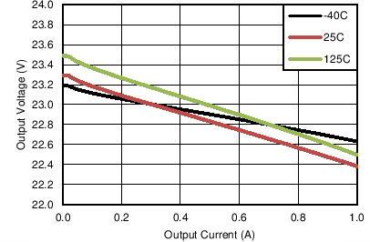 Figure 1. VOH vs IOH
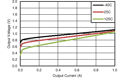 Figure 2. VOL vs IOL