SCES274I May 1999 – October 2014 SN74LVCZ244A
PRODUCTION DATA.
- 1 Features
- 2 Applications
- 3 Description
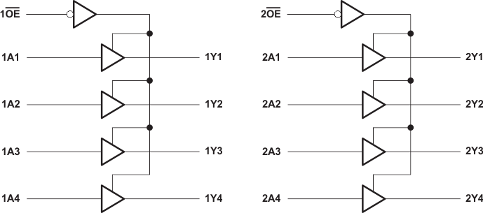
- 4 Simplified Schematic
- 5 Revision History
- 6 Pin Configuration and Functions
- 7 Specifications
- 8 Parameter Measurement Information
- 9 Detailed Description
- 10Application and Implementation
- 11Power Supply Recommendations
- 12Layout
- 13Device and Documentation Support
- 14Mechanical, Packaging, and Orderable Information
封装选项
请参考 PDF 数据表获取器件具体的封装图。
机械数据 (封装 | 引脚)
- DB|20
- NS|20
- PW|20
- DW|20
散热焊盘机械数据 (封装 | 引脚)
- PW|20
订购信息
9 Detailed Description
9.1 Overview
This octal buffer/line driver is designed for 2.7-V to 3.6-V VCC operation.
The SN74LVCZ244A device is organized as two 4-bit line drivers with separate output-enable (OE) inputs. When OE is low, the device passes data from the A inputs to the Y outputs. When OE is high, the outputs are in the high-impedance state.
Inputs can be driven from either 3.3-V or 5-V devices. This feature allows the use of this device as a translator in a mixed 3.3-V/5-V system environment.
When VCC is between 0 and 1.5 V, the device is in the high-impedance state during power up or power down. However, to ensure the high-impedance state above 1.5 V, OE should be tied to VCC through a pullup resistor; the minimum value of the resistor is determined by the current-sinking capability of the driver.
This device is fully specified for hot-insertion applications using Ioff and power-up 3-state. The Ioff circuitry disables the outputs, preventing damaging current backflow through the device when it is powered down. The power-up 3-state circuitry places the outputs in the high-impedance state during power up and power down, which prevents driver conflict.
9.2 Functional Block Diagram
9.3 Feature Description
- Wide operating voltage range
- Operates from 2.7 V to 3.6 V
- Allows down-voltage translation
- Inputs accept voltages to 5.5 V
- Ioff feature
- Allows voltages on the inputs and outputs when VCC is 0 V
- Power-up 3-state feature
- Keeps the outputs in high impedance during power up and allows for hot insertion
9.4 Device Functional Modes
Table 1. Function Table
| INPUTS | OUTPUTS Y |
|
|---|---|---|
| OE | A | |
| L | H | H |
| L | L | L |
| H | X | High-Z |