SCAS572L April 1996 – July 2014 SN74LVC2244A
PRODUCTION DATA.
- 1 Features
- 2 Applications
- 3 Description
- 4 Simplified Schematic
- 5 Revision History
- 6 Pin Configuration and Functions
- 7 Specifications
- 8 Detailed Description
- 9 Application and Implementation
- 10Power Supply Recommendations
- 11Layout
- 12Device and Documentation Support
- 13Mechanical, Packaging, and Orderable Information
封装选项
请参考 PDF 数据表获取器件具体的封装图。
机械数据 (封装 | 引脚)
- DGV|20
- DB|20
- DBQ|20
- NS|20
- DW|20
- PW|20
散热焊盘机械数据 (封装 | 引脚)
- PW|20
订购信息
9 Application and Implementation
9.1 Application Information
Inputs can be driven from either 3.3-V or 5-V devices. This feature allows the use of this device as a translator in a mixed 3.3-V/5-V system environment. This device is fully specified for partial-power-down applications using Ioff. The Ioff circuitry disables the outputs, preventing damaging current backflow through the device when it is powered down. To ensure the high-impedance state during power up or power down, OE should be tied to VCC through a pullup resistor; the minimum value of the resistor is determined by the current-sinking capability of the driver.
9.2 Typical Application
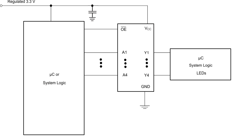 Figure 4. Typical Application Diagram
9.2.1 Design Requirements
This device uses CMOS technology and has balanced output drive. Care should be taken to avoid bus contention because it can drive currents that would exceed maximum limits. The high drive will also create fast edges into light loads, so routing and load conditions should be considered to prevent ringing.
9.2.2 Detailed Design Procedure
- Recommended Input Conditions
- Rise time and fall time specs: See (Δt/ΔV) in the Recommended Operating Conditions table.
- Specified high and low levels: See (VIH and VIL) in the Recommended Operating Conditions table.
- Inputs are overvoltage tolerant allowing them to go as high as 5.5 V at any valid VCC.
- Recommend Output Conditions
- Load currents should not exceed 25 mA per output and 50 mA total for the part.
- Outputs should not be pulled above VCC.
9.2.3 Application Curves
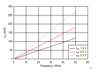 Figure 5. ICC vs Frequency