SCLS469F March 2003 – December 2014 SN74LV4052A-Q1
PRODUCTION DATA.
- 1 Features
- 2 Applications
- 3 Description
- 4 Revision History
- 5 Pin Configuration and Functions
- 6 Specifications
- 7 Parameter Measurement Information
- 8 Detailed Description
- 9 Application and Implementation
- 10Power Supply Recommendations
- 11Layout
- 12Device and Documentation Support
- 13Mechanical, Packaging, and Orderable Information
封装选项
机械数据 (封装 | 引脚)
散热焊盘机械数据 (封装 | 引脚)
- D|16
订购信息
5 Pin Configuration and Functions
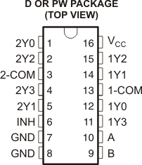
Pin Functions
| PIN | I/O(1) | DESCRIPTION | |
|---|---|---|---|
| NO. | NAME | ||
| 1 | 2Y0 | I(1) | Input to mux 2 |
| 2 | 2Y2 | I(1) | Input to mux 2 |
| 3 | 2-COM | O(1) | Output of mux 2 |
| 4 | 2Y3 | I(1) | Input to mux 2 |
| 5 | 2Y1 | I(1) | Input to mux 2 |
| 6 | INH | I | Enables the outputs of the device. Logic low level with turn the outputs on, high level will turn them off. |
| 7 | GND | - | Ground |
| 8 | GND | - | Ground |
| 9 | B | I | Selector line for outputs (see Device Functional Modes for specific information) |
| 10 | A | I | Selector line for outputs (see Device Functional Modes for specific information) |
| 11 | 1Y3 | I(1) | Input to mux 1 |
| 12 | 1Y0 | I(1) | Input to mux 1 |
| 13 | 1-COM | O(1) | Output of mux 1 |
| 14 | 1Y1 | I(1) | Input to mux 1 |
| 15 | 1Y2 | I(1) | Input to mux 1 |
| 16 | Vcc | I | Device power input |
(1) These I/O descriptions represent the device when used as a multiplexer, when this device is operated as a demultiplexer pins 1Y0, 1Y1, 1Y2, 1Y3, 2Y0, 2Y1, 2Y2, 2Y3 may be considered outputs (O) and pins 1-COM and 2-COM may be considered inputs (I).