ZHCSQR1R April 1998 – March 2023 SN74LV165A
PRODMIX
- 1 特性
- 2 应用
- 3 说明
- 4 Revision History
- 5 Pin Configuration and Functions
-
6 Specifications
- 6.1 Absolute Maximum Ratings
- 6.2 ESD Ratings
- 6.3 Recommended Operating Conditions
- 6.4 Thermal Information
- 6.5 Electrical Characteristics
- 6.6 Timing Requirements, VCC = 2.5 V ± 0.2 V
- 6.7 Timing Requirements, VCC = 3.3 V ± 0.3 V
- 6.8 Timing Requirements, VCC = 5 V ± 0.5 V
- 6.9 Switching Characteristics, VCC = 2.5 V ± 0.2 V
- 6.10 Switching Characteristics, VCC = 3.3 V ± 0.3 V
- 6.11 Switching Characteristics,VCC = 5 V ± 0.5 V
- 6.12 Timing Diagrams
- 6.13 Operating Characteristics
- 6.14 Typical Characteristics
- 7 Parameter Measurement Information
- 8 Detailed Description
- 9 Application and Implementation
- 10Device and Documentation Support
- 11Mechanical, Packaging, and Orderable Information
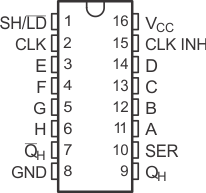
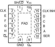
5 Pin Configuration and Functions
 Figure 5-1 D, DB, DGV, N or PW Package,
16-Pin SOIC, SSOP, TVSOP, SOP or TSSOP
(Top View)
 Figure 5-2 RGY or BQB
Package,
Figure 5-2 RGY or BQB
Package,16-Pin VQFN or WQFN
(Top View)
Table 5-1 Pin Functions
| PIN | TYPE (1) | DESCRIPTION | |
|---|---|---|---|
| NAME | NO. | ||
| A | 11 | I | Serial input A |
| B | 12 | I | Serial input B |
| C | 13 | I | Serial input C |
| CLK | 2 | I | Storage clock |
| CLK INH | 15 | I | Storage clock |
| D | 14 | I | Serial input D |
| E | 3 | I | Serial input E |
| F | 4 | I | Serial input F |
| G | 5 | I | Serial input G |
| GND | 8 | G | Ground pin |
| H | 6 | I | Serial input H |
| QH | 7 | O | Output H, inverted |
| QH | 9 | O | Output H |
| SH/ LD | 1 | I | Load Input |
| SER | 10 | I | Serial input |
| VCC | 16 | P | Power pin |
| PAD | — | Thermal Pad(2) | |
(1) I = Input, O = Output, I/O = Input or Output, G = Ground, P = Power.
(2) RGY and BQB Package Only