SDLS146B October 1976 – September 2016 SN54LS245 , SN74LS245
- 1 Features
- 2 Applications
- 3 Description
- 4 Revision History
- 5 Device Comparison Table
- 6 Pin Configuration and Functions
- 7 Specifications
- 8 Parameter Measurement Information
- 9 Detailed Description
- 10Application and Implementation
- 11Power Supply Recommendations
- 12Layout
- 13Device and Documentation Support
- 14Mechanical, Packaging, and Orderable Information
封装选项
请参考 PDF 数据表获取器件具体的封装图。
机械数据 (封装 | 引脚)
- DB|20
- NS|20
- N|20
- DW|20
散热焊盘机械数据 (封装 | 引脚)
订购信息
12 Layout
12.1 Layout Guidelines
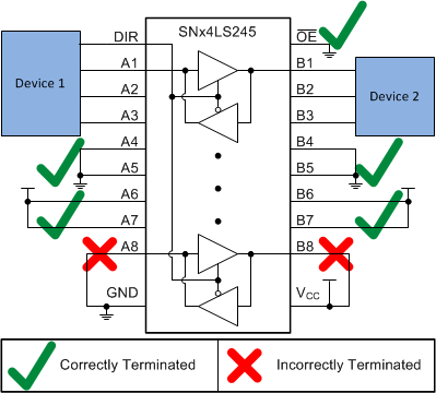
When using multiple bit logic devices, inputs must not be left floating. In many applications, some channels of the SNx4LS245 are unused, and thus must be terminated properly. Because each transceiver channel pin can be either an input or an output, they must be treated as both when being terminated. Ground or VCC (whichever is more convenient) can be used to terminate unused inputs; however, each unused channel should be terminated to the same logic level on both the A and B side. For example, in Figure 7 unused channels 4, 5, 6, and 7 are terminated correctly with both sides connected to the same voltage, while channel 8 is terminated incorrectly with each side being tied to a different voltage. The OE input is also unused in this example, and is terminated directly to ground to permanently enable all outputs.
12.2 Layout Example
 Figure 7. Example Demonstrating How to Terminate Unused Inputs and Channels of a Transceiver