SCES582H July 2004 – April 2015 SN74AVCH2T45
PRODUCTION DATA.
- 1 Features
- 2 Applications
- 3 Description
- 4 Revision History
- 5 Description (Continued)
- 6 Pin Configurations and Functions
-
7 Specifications
- 7.1 Absolute Maximum Ratings
- 7.2 ESD Ratings
- 7.3 Recommended Operating Conditions
- 7.4 Thermal Information
- 7.5 Electrical Characteristics
- 7.6 Switching Characteristics: VCCA = 1.2 V
- 7.7 Switching Characteristics: VCCA = 1.5 V
- 7.8 Switching Characteristics: VCCA = 1.8 V
- 7.9 Switching Characteristics: VCCA = 2.5 V
- 7.10 Switching Characteristics: VCCA = 3.3 V
- 7.11 Operating Characteristics
- 7.12 Typical Characteristics
- 8 Parameter Measurement Information
- 9 Detailed Description
- 10Application and Implementation
- 11Power Supply Recommendations
- 12Layout
- 13Device and Documentation Support
- 14Mechanical, Packaging, and Orderable Information
封装选项
请参考 PDF 数据表获取器件具体的封装图。
机械数据 (封装 | 引脚)
- DCU|8
- YZP|8
- DCT|8
散热焊盘机械数据 (封装 | 引脚)
订购信息
6 Pin Configurations and Functions
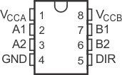
DCT and DCU Packages
8-Pin SSOP and VSSOP
Top View

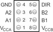
YZP Package
8-Pin DSBGA
Bottom View

Pin Functions
| PIN | DESCRIPTION | ||
|---|---|---|---|
| NAME | SSOP, VSSOP |
DSBGA | |
| VCCA | 1 | A1 | Supply Voltage A |
| VCCB | 8 | A2 | Supply Voltage B |
| GND | 4 | D1 | Ground |
| A1 | 2 | B1 | Output or input depending on state of DIR. Output level depends on VCCA. |
| A2 | 3 | C1 | Output or input depending on state of DIR. Output level depends on VCCA. |
| B1 | 7 | B2 | Output or input depending on state of DIR. Output level depends on VCCB. |
| B2 | 6 | C2 | Output or input depending on state of DIR. Output level depends on VCCB. |
| DIR | 5 | D2 | Direction Pin, Connect to GND or to VCCA. |