SCES592I July 2004 – September 2017 SN74AUP1G79
PRODUCTION DATA.
- 1 Features
- 2 Applications
- 3 Description
- 4 Revision History
- 5 Pin Configuration and Functions
-
6 Specifications
- 6.1 Absolute Maximum Ratings
- 6.2 ESD Ratings
- 6.3 Recommended Operating Conditions
- 6.4 Thermal Information
- 6.5 Electrical Characteristics: TA = 25°C
- 6.6 Electrical Characteristics: TA = -40°C to 85°C
- 6.7 Timing Requirements
- 6.8 Switching Characteristics: CL = 5 pF
- 6.9 Switching Characteristics: CL = 10 pF
- 6.10 Switching Characteristics: CL = 15 pF
- 6.11 Switching Characteristics: CL = 30 pF
- 6.12 Operating Characteristics
- 6.13 Typical Characteristics
- 7 Parameter Measurement Information
- 8 Detailed Description
- 9 Applications, Implementation, and Layout
- 10Power Supply Recommendations
- 11Layout
- 12Device and Documentation Support
- 13Mechanical, Packaging, and Orderable Information
封装选项
机械数据 (封装 | 引脚)
散热焊盘机械数据 (封装 | 引脚)
订购信息
9 Applications, Implementation, and Layout
NOTE
Information in the following applications sections is not part of the TI component specification, and TI does not warrant its accuracy or completeness. TI’s customers are responsible for determining suitability of components for their purposes. Customers should validate and test their design implementation to confirm system functionality.
9.1 Application Information
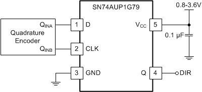
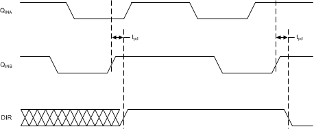
A rotary quadrature encoder is a simple, infinitely-turning knob that outputs two out-of-phase square waves as it is turned and is often used in electronics as a method of human interface. One signal will lead the other in phase depending on which direction the knob is turned. The SN74AUP1G79 can be used to determine which direction the knob is being turned without the need for a microcontroller or other complex monitoring system by connecting the outputs of the knob to the D and CLK inputs of the SN74AUP1G79 as shown in Figure 7. It is important to note that the CLK input will control when the direction signal changes, as shown in Figure 8.
9.2 Typical Application
 Figure 7. Typical Application Diagram
 Figure 8. Timing Diagram for Quadrature Encoder Application
9.2.1 Design Requirements
The SN74AUP1G79 device uses CMOS technology and has balanced output drive. Take care to avoid bus contention because it can drive currents that would exceed maximum limits.
9.2.2 Detailed Design Procedure
- Recommended Input conditions
- Rise time and fall time specifications. See Δt/ΔV in Recommended Operating Conditions.
- Specified high and low levels. See VIH and VIL in Recommended Operating Conditions.
- Inputs are overvoltage tolerant, which allows them to go as high as 3.6 V at any valid VCC
- Recommended output conditions
- Load currents must not exceed 20 mA on the output and 50 mA total for the part
9.2.3 Application Curves

