SCES375P september 2001 – June 2017 SN74AUC1G14
UNLESS OTHERWISE NOTED, this document contains PRODUCTION DATA.
- 1 Features
- 2 Applications
- 3 Description
- 4 Revision History
- 5 Pin Configuration and Functions
- 6 Specifications
- 7 Parameter Measurement Information
- 8 Detailed Description
- 9 Device and Documentation Support
- 10Mechanical, Packaging, and Orderable Information
封装选项
请参考 PDF 数据表获取器件具体的封装图。
机械数据 (封装 | 引脚)
- DBV|5
- DCK|5
散热焊盘机械数据 (封装 | 引脚)
订购信息
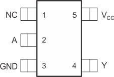
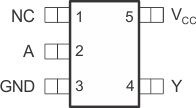
5 Pin Configuration and Functions
DBV Package
5-Pin SOT-23
Top View

DCK Package
5-Pin SC70
Top View

YZP Package
5-Pin DSBGA
Bottom View

See mechanical drawings for dimensions.
DNU – Do not use
NC – No internal connection
Pin Functions
| PIN | I/O | DESCRIPTION | ||
|---|---|---|---|---|
| NAME | DBV, DCK | YZP | ||
| A | 2 | B1 | I | Logic input |
| DNU | — | A1 | — | Do not use |
| GND | 3 | C1 | — | Ground |
| NC | 1 | — | — | No internal connection |
| VCC | 5 | A2 | — | Positive supply |
| Y | 4 | C2 | O | Inverted output |