ZHCSJ17H November 2002 – November 2018 SN65HVD233 , SN65HVD234 , SN65HVD235
PRODUCTION DATA.
- 1 特性
- 2 应用
- 3 说明
- 4 修订历史记录
- 5 (说明 (续))
- 6 Device Comparison Table
- 7 Pin Configuration and Functions
-
8 Specifications
- 8.1 Absolute Maximum Ratings
- 8.2 ESD Ratings
- 8.3 Recommended Operating Conditions
- 8.4 Thermal Information
- 8.5 Power Dissipation Ratings
- 8.6 Electrical Characteristics: Driver
- 8.7 Electrical Characteristics: Receiver
- 8.8 Switching Characteristics: Driver
- 8.9 Switching Characteristics: Receiver
- 8.10 Switching Characteristics: Device
- 8.11 Typical Characteristics
- 9 Parameter Measurement Information
- 10Detailed Description
- 11Application and Implementation
- 12Power Supply Recommendations
- 13Layout
- 14器件和文档支持
- 15机械、封装和可订购信息
11.3.1.2 Differential Signal
CAN is a differential bus where complementary signals are sent over two wires and the voltage difference between the two wires defines the logical state of the bus. The differential CAN receiver monitors this voltage difference and outputs the bus state with a single ended logic level output signal.
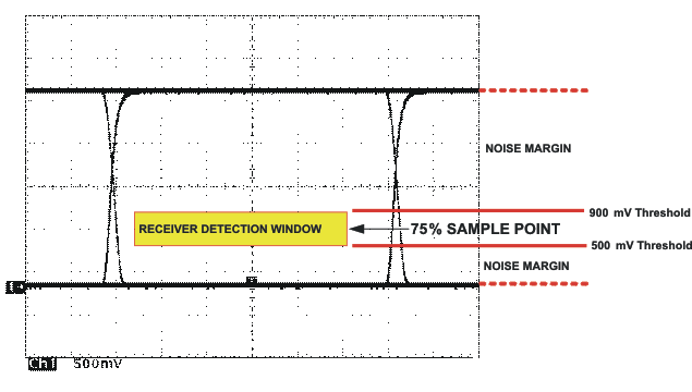
 Figure 40. Typical SN65HVD230 Differential Output Voltage Waveform
 The CAN driver creates the differential voltage between CANH and CANL in the dominant state. The dominant differential output of the SN65HVD23x is greater than 1.5 V and less than 3 V across a 60 ohm load as defined by the ISO 11898 standard. These are the same limiting values for 5 V supplied CAN transceivers. The bus termination resistors drive the recessive bus state and not the CAN driver.
A CAN receiver is required to output a recessive state when less than 500 mV of differential voltage exists on the bus, and a dominant state when more than 900 mV of differential voltage exists on the bus. The CAN receiver must do this with common-mode input voltages from –2 V to 7 V. The SN65HVD23x family receivers meet these same input specifications as 5 V supplied receivers.