SLLSE49D September 2010 – July 2017 SN65HVD1780-Q1 , SN65HVD1781-Q1 , SN65HVD1782-Q1
UNLESS OTHERWISE NOTED, this document contains PRODUCTION DATA.
- 1 Features
- 2 Applications
- 3 Description
- 4 Revision History
- 5 Pin Configuration and Functions
- 6 Specifications
- 7 Parameter Measurement Information
- 8 Detailed Description
- 9 Application and Implementation
- 10Power Supply Recommendations
- 11Layout
- 12Device and Documentation Support
- 13Mechanical, Packaging, and Orderable Information
7 Parameter Measurement Information
Input generator rate is 100 kbps, 50% duty cycle, rise and fall times less than 6 ns, output impedance 50 Ω.
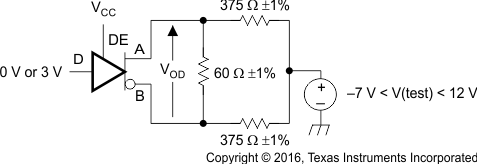
 Figure 6. Measurement of Driver Differential Output Voltage With Common-Mode Load
 Figure 7. Measurement of Driver Differential and Common-Mode Output With RS-485 Load
 Figure 8. Measurement of Driver Differential Output Rise and Fall Times and Propagation Delays

NOTE:
D at 3 V to test non-inverting output, D at 0 V to test inverting output.
NOTE:
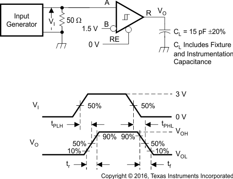
D at 0 V to test non-inverting output, D at 3 V to test inverting output. Figure 11. Measurement of Receiver Output Rise and Fall Times and Propagation Delays
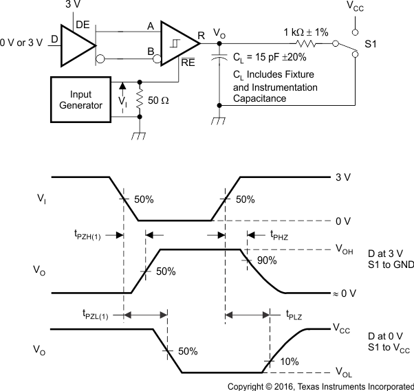
 Figure 12. Measurement of Receiver Enable and Disable Times With Driver Enabled
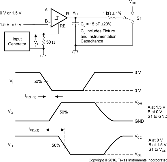
 Figure 13. SN65HVD1781 Measurement of Receiver Enable Times With Driver Disabled