SLLS934F November 2008 – November 2015 SN65HVD11-HT
PRODUCTION DATA.
- 1 Features
- 2 Applications
- 3 Description
- 4 Revision History
- 5 Pin Configuration and Functions
- 6 Specifications
- 7 Parameter Measurement Information
- 8 Detailed Description
- 9 Application and Implementation
- 10Power Supply Recommendations
- 11Layout
- 12Device and Documentation Support
- 13Mechanical, Packaging, and Orderable Information
封装选项
机械数据 (封装 | 引脚)
散热焊盘机械数据 (封装 | 引脚)
订购信息
7 Parameter Measurement Information
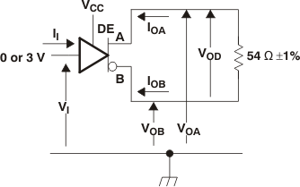 Figure 10. Driver VOD Test Circuit and Voltage and Current Definitions
 Figure 11. Driver VOD With Common Mode Loading Test Circuit
 Figure 12. Test Circuit and Definitions for Driver Common Mode Output Voltage
 Figure 13. Driver Switching Test Circuit and Voltage Waveforms
 Figure 14. Driver High-Level Enable and Disable Time Test Circuit and Voltage Waveforms
 Figure 15. Driver Low-Level Output Enable and Disable Time Test Circuit and Voltage Waveforms
 Figure 16. Receiver Voltage and Current Definitions
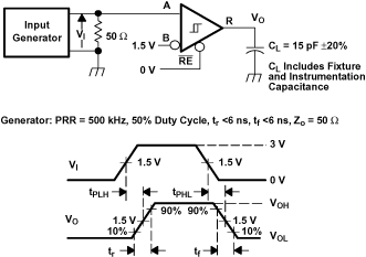 Figure 17. Receiver Switching Test Circuit and Voltage Waveforms
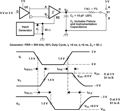 Figure 18. Receiver Enable and Disable Time Test Circuit and Voltage Waveforms With Drivers Enabled
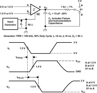 Figure 19. Receiver Enable Time From Standby (Driver Disabled)
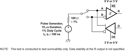 Figure 20. Test Circuit, Transient Overvoltage Test
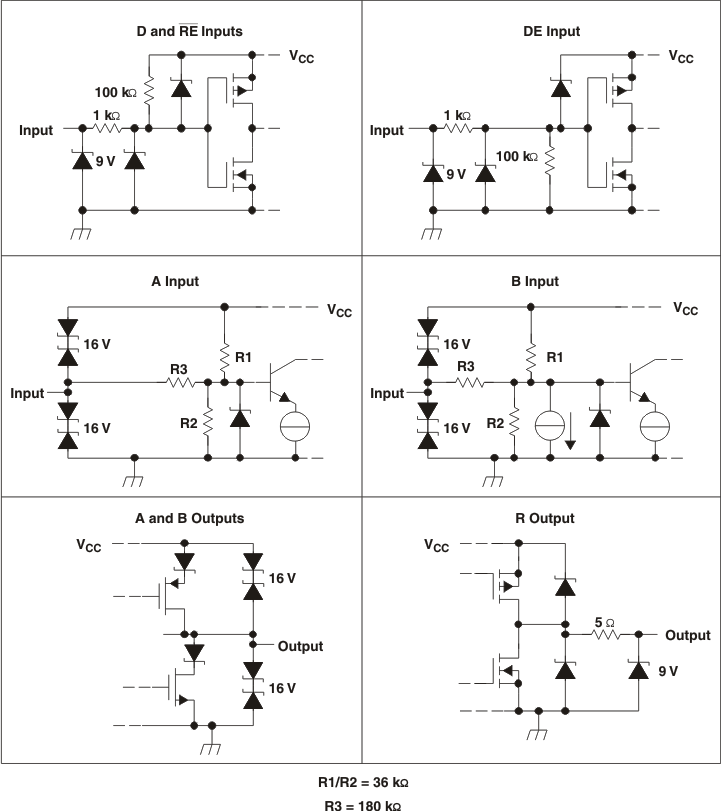 Figure 21. Equivalent Input and Output Schematic Diagrams