SLRS021D December 1967 – January 2017 SN55451B , SN55452B , SN55453B , SN55454B , SN75451B , SN75452B , SN75453B , SN75454B
PRODUCTION DATA.
- 1 Features
- 2 Applications
- 3 Description
- 4 Revision History
- 5 Device Comparison Table
- 6 Pin Configuration and Functions
- 7 Specifications
- 8 Parameter Measurement Information
- 9 Detailed Description
- 10Application and Implementation
- 11Power Supply Recommendations
- 12Layout
- 13Device and Documentation Support
- 14Mechanical, Packaging, and Orderable Information
封装选项
请参考 PDF 数据表获取器件具体的封装图。
机械数据 (封装 | 引脚)
- FK|20
- JG|8
散热焊盘机械数据 (封装 | 引脚)
订购信息
10 Application and Implementation
NOTE
Information in the following applications sections is not part of the TI component specification, and TI does not warrant its accuracy or completeness. TI’s customers are responsible for determining suitability of components for their purposes. Customers should validate and test their design implementation to confirm system functionality.
10.1 Application Information
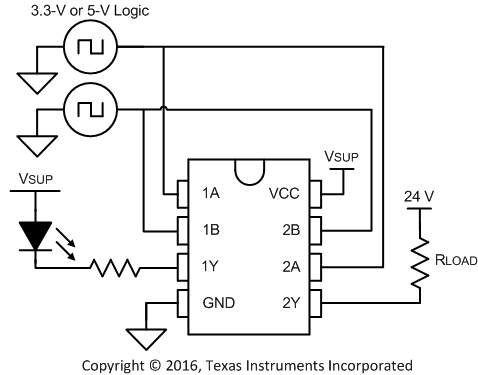
Typically the SN75451B device drives a high-voltage or high-current peripheral from an MCU or logic device that cannot tolerate these conditions. The following design is a common application of the SN75451B device, driving an LED using one channel and a high voltage peripheral using the other. In this configuration, the LED will turn on whenever the high voltage peripheral is on.
10.2 Typical Application
 Figure 18. SN75451B Driving an LED and a High Voltage Peripheral
10.2.1 Design Requirements
Each of the inputs to the logic gate should never float. If one of the inputs is floating, then the logic gate could be in an unknown state. Be sure to connect ground or VCC to any unused input channels.
10.2.2 Detailed Design Procedure
- Recommended Input Conditions:
- For specified high and low levels, see VIH and VIL in Recommended Operating Conditions.
- The input voltage must not exceed the VI specified in Absolute Maximum Ratings.
- Recommended Output Conditions:
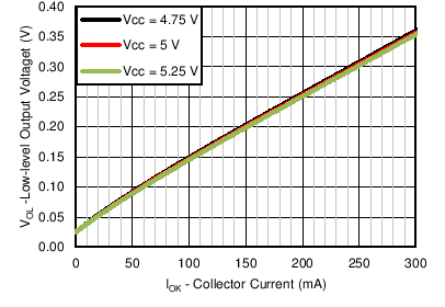
- It is recommended that the load current not exceed 300 mA.
- The load current must never exceed the IOK noted in Absolute Maximum Ratings.
10.2.3 Application Curves
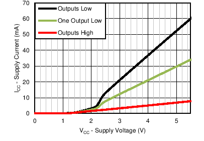
 Figure 19. SN75451B Typical Supply Current vs Supply Voltage
 Figure 20. SN75451B Typical Low-Level Output Voltage vs Collector Current