SBOS502F September 2009 – December 2016 REF5025-HT
PRODUCTION DATA.
- 1 Features
- 2 Applications
- 3 Description
- 4 Revision History
- 5 Pin Configuration and Functions
- 6 Specifications
- 7 Detailed Description
- 8 Application and Implementation
- 9 Power Supply Recommendations
- 10Layout
- 11Device and Documentation Support
- 12Mechanical, Packaging, and Orderable Information
封装选项
机械数据 (封装 | 引脚)
散热焊盘机械数据 (封装 | 引脚)
订购信息
10 Layout
10.1 Layout Guidelines
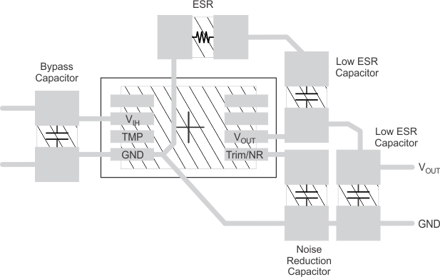
- Place the power-supply bypass capacitor as closely as possible to the VIN pin and ground pins. TI recommends a bypass capacitor value of 1 μF to 10 μF. If necessary, additional decoupling capacitance can be added to compensate for noisy or high-impedance power supplies.
- Place a 1-µF noise filtering capacitor between the NR pin and ground.
- The output must be decoupled with a 1-µF to 50-µF capacitor. In series with the load capacitor, add an ESR of 1-Ω for the best noise performance.
- A high-frequency, 1-µF capacitor can be added in parallel between the output and ground to filter noise and help with switching loads as data converters.
10.2 Layout Example
 Figure 37. Recommended Layout for REF5025-HT
10.3 Power Dissipation
The REF50xx family is specified to deliver current loads of ±10-mA over the specified input voltage range. The temperature of the device increases according to Equation 3:
Equation 3. TJ = TA + PD × RθJA
where
- TJ = Junction temperature (°C)
- TA = Ambient temperature (°C)
- PD = Power dissipated (W)
- RθJA = Junction-to-ambient thermal resistance (°C/W)
The REF50xx junction temperature must not exceed the absolute maximum rating of +150°C.