SBOS471B April 2010 – June 2015 REF5020-EP , REF5025-EP , REF5040-EP , REF5050-EP
PRODUCTION DATA.
- 1 Features
- 2 Applications
- 3 Description
- 4 Revision History
- 5 Pin Configuration and Functions
- 6 Specifications
- 7 Detailed Description
- 8 Application and Implementation
- 9 Power Supply Recommendations
- 10Layout
- 11Device and Documentation Support
- 12Mechanical, Packaging, and Orderable Information
9 Power Supply Recommendations
The maximum voltage drop between the input and output pin is 0.2 V. The minimum power supply voltage for the specific REF50xx device depends on the value of the output voltage, (VINMIN = VOUT + 0.2 V). The exception to this rule is the REF5020, which requires a minimum 2.7-V power supply for proper operation. The maximum power supply voltage for the REF50xx series is 18 V. TI recommends adding a bypass capacitor of 1 μF to 10 μF at the input to compensate for the layout and power supply source impedance.
9.1 Basic Connections
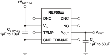
Figure 34 shows the typical connections for the REF50xx. TI recommends a supply bypass capacitor ranging from 1 μF to 10 μF. A 1-μF to 50-μF output capacitor (CL) must be connected from VOUT to GND. The ESR value of CL must be less than or equal to 1.5 Ω to ensure output stability. To minimize noise, the recommended ESR of CL is between 1 Ω and 1.5 Ω.
 Figure 34. Basic Connections
9.2 Low Dropout Voltage
The REF50xx family of voltage references features extremely low dropout voltage. With the exception of the REF5020, which has a minimum supply requirement of 2.7 V, these references can be operated with a supply of 200 mV above the output voltage in an unloaded condition. For loaded conditions, a typical dropout voltage versus load plot is shown in Figure 6 in Typical Characteristics.