ZHCSDH3 November   2014 PCM5252

PRODUCTION DATA.  

  1. 特性
  2. 应用
  3. 说明
  4. 修订历史记录
  5. Device Comparison
  6. Pin Configuration and Functions
    1. 6.1 Control Mode Effect On Pin Assignments
    2. 6.2 Pin Assignments
  7. Specifications
    1. 7.1  Absolute Maximum Ratings
    2. 7.2  ESD Ratings
    3. 7.3  Recommended Operating Conditions
    4. 7.4  Thermal Information
    5. 7.5  Electrical Characteristics
    6. 7.6  Switching Characteristics
    7. 7.7  Timing Requirements: SCK Input
    8. 7.8  Timing Requirements: PCM Audio Data
    9. 7.9  Timing Requirements: I2S Master, See
    10. 7.10 Timing Requirements: XSMT
    11. 7.11 Typical Characteristics
  8. Detailed Description
    1. 8.1 Overview
    2. 8.2 Functional Block Diagram
    3. 8.3 Feature Description
      1. 8.3.1 Terminology
      2. 8.3.2 Audio Data Interface
        1. 8.3.2.1 Audio Serial Interface
        2. 8.3.2.2 PCM Audio Data Formats
        3. 8.3.2.3 Zero Data Detect
      3. 8.3.3 XSMT Pin (Soft Mute / Soft Un-Mute)
      4. 8.3.4 Audio Processing
        1. 8.3.4.1  PCM5252 Audio Processing Options
          1. 8.3.4.1.1 Overview
          2. 8.3.4.1.2 miniDSP Instruction Register
          3. 8.3.4.1.3 Digital Output
          4. 8.3.4.1.4 Software
        2. 8.3.4.2  Interpolation Filter
        3. 8.3.4.3  Overview
        4. 8.3.4.4  Smart SOA
        5. 8.3.4.5  Smart BASS
        6. 8.3.4.6  Smart Protection
        7. 8.3.4.7  Implementing a Real World Design
        8. 8.3.4.8  Digital Output
        9. 8.3.4.9  Software
        10. 8.3.4.10 Process Flow
      5. 8.3.5 DAC and Differential Analog Outputs
        1. 8.3.5.1 Analog Outputs
        2. 8.3.5.2 Choosing Between VREF and VCOM Modes
          1. 8.3.5.2.1 Voltage Reference and Output Levels
          2. 8.3.5.2.2 Mode Switching Sequence, from VREF Mode to VCOM Mode
        3. 8.3.5.3 Digital Volume Control
          1. 8.3.5.3.1 Emergency Ramp-Down
        4. 8.3.5.4 Analog Gain Control
      6. 8.3.6 Reset and System Clock Functions
        1. 8.3.6.1 Clocking Overview
        2. 8.3.6.2 Clock Slave Mode With Master and System Clock (SCK) Input (4 Wire I2S)
        3. 8.3.6.3 Clock Slave Mode With BCK PLL to Generate Internal Clocks (3-Wire PCM)
        4. 8.3.6.4 Clock Generation Using the PLL
        5. 8.3.6.5 PLL Calculation
          1. 8.3.6.5.1 Examples:
            1. 8.3.6.5.1.1 Recommended PLL Settings
        6. 8.3.6.6 Clock Master Mode from Audio Rate Master Clock
        7. 8.3.6.7 Clock Master from a Non-Audio Rate Master Clock
    4. 8.4 Device Functional Modes
      1. 8.4.1 Choosing a Control Mode
        1. 8.4.1.1 Software Control
          1. 8.4.1.1.1 SPI Interface
            1. 8.4.1.1.1.1 Register Read and Write Operation
          2. 8.4.1.1.2 I2C Interface
            1. 8.4.1.1.2.1 Slave Address
            2. 8.4.1.1.2.2 Register Address Auto-Increment Mode
            3. 8.4.1.1.2.3 Packet Protocol
            4. 8.4.1.1.2.4 Write Register
            5. 8.4.1.1.2.5 Read Register
            6. 8.4.1.1.2.6 Timing Characteristics
      2. 8.4.2 VREF and VCOM Modes
  9. Application and Implementation
    1. 9.1 Application Information
    2. 9.2 Typical Application
      1. 9.2.1 High Fidelity Smartphone Application
        1. 9.2.1.1 Design Requirements
        2. 9.2.1.2 Detailed Design Procedure
          1. 9.2.1.2.1 Initialization Script
        3. 9.2.1.3 Application Performance Plot
  10. 10Power Supply Recommendations
    1. 10.1 Power Supply Distribution and Requirements
    2. 10.2 Recommended Powerdown Sequence
      1. 10.2.1 XSMT = 0
      2. 10.2.2 Clock Error Detect
      3. 10.2.3 Planned Shutdown
      4. 10.2.4 Unplanned Shutdown
    3. 10.3 External Power Sense Undervoltage Protection Mode
    4. 10.4 Power-On Reset Function
      1. 10.4.1 Power-On Reset, DVDD 3.3-V Supply
      2. 10.4.2 Power-On Reset, DVDD 1.8-V Supply
    5. 10.5 PCM5252 Power Modes
      1. 10.5.1 Setting Digital Power Supplies and I/O Voltage Rails
      2. 10.5.2 Power Save Modes
      3. 10.5.3 Power Save Parameter Programming
  11. 11Layout
    1. 11.1 Layout Guidelines
    2. 11.2 Layout Example
  12. 12Programming
    1. 12.1 Coefficient Data Formats
    2. 12.2 Power Down and Reset Behavior
  13. 13Register Maps
    1. 13.1 PCM5252 Register Map
      1. 13.1.1 Detailed Register Descriptions
        1. 13.1.1.1 Register Map Summary
        2. 13.1.1.2 Page 0 Registers
        3. 13.1.1.3 Page 1 Registers
        4. 13.1.1.4 Page 44 Registers
        5. 13.1.1.5 Page 253 Registers
      2. 13.1.2 PLL Tables for Software Controlled Devices
  14. 14器件和文档支持
    1. 14.1 社区资源
    2. 14.2 商标
    3. 14.3 静电放电警告
  15. 15机械、封装和可订购信息

封装选项

机械数据 (封装 | 引脚)
散热焊盘机械数据 (封装 | 引脚)
订购信息

Layout

Layout Guidelines

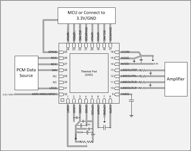
  • The PCM5252 family of devices are simple to layout. Most engineers use a shared common ground for an entire device. GND can consider AGND and DGND connected.
  • Good system partitioning should keep digital clock and interface traces away from the differential analog outputs for highest analog performance. This reduces any high-speed clock return currents influencing the analog outputs.
  • Power supply and charge pump decoupling capacitors should be placed as close as possible to the device.
  • The thermal pad on the underside of the package should be connected to GND.
  • The top layer should be used for routing signals, whilst the bottom layer can be used for GND.

Layout Example

PCM5252 layout_slase12.gif Figure 83. PCM5252 Layout Example