ZHCSOM7G July   2001  – August 2021 PCF8574A

PRODUCTION DATA  

  1. 特性
  2. 应用
  3. 说明
  4. Revision History
  5. Pin Configuration and Functions
  6. Specifications
    1. 6.1 Absolute Maximum Ratings
    2. 6.2 ESD Ratings
    3. 6.3 Recommended Operating Conditions
    4. 6.4 Thermal Information
    5. 6.5 Electrical Characteristics
    6. 6.6 I2C Interface Timing Requirements
    7. 6.7 Switching Characteristics
    8. 6.8 Typical Characteristics
  7. Parameter Measurement Information
  8. Detailed Description
    1. 8.1 Overview
    2. 8.2 Functional Block Diagram
      1. 8.2.1 Simplified Block Diagram of Device
      2. 8.2.2 Simplified Schematic Diagram of Each P-Port Input/Output
    3. 8.3 Feature Description
      1. 8.3.1 I2C Interface
      2. 8.3.2 Interface Definition
      3. 8.3.3 Address Reference
    4. 8.4 Device Functional Modes
  9. Application Information Disclaimer
    1. 9.1 Application Information
    2. 9.2 Typical Application
      1. 9.2.1 Design Requirements
        1. 9.2.1.1 Minimizing ICC When I/Os Control LEDs
      2. 9.2.2 Detailed Design Procedure
      3. 9.2.3 Application Curves
  10. 10Power Supply Recommendations
    1. 10.1 Power-On Reset Requirements
  11. 11Layout
    1. 11.1 Layout Guidelines
    2. 11.2 Layout Example
  12. 12Device and Documentation Support
    1. 12.1 Documentation Support
      1. 12.1.1 Glossary
    2. 12.2 Receiving Notification of Documentation Updates
    3. 12.3 支持资源
    4. 12.4 Trademarks
    5. 12.5 静电放电警告
    6. 12.6 术语表
  13. 13Mechanical, Packaging, and Orderable Information

封装选项

请参考 PDF 数据表获取器件具体的封装图。

机械数据 (封装 | 引脚)
  • DGV|20
  • DW|16
  • N|16
  • PW|20
  • RGY|20
散热焊盘机械数据 (封装 | 引脚)
订购信息

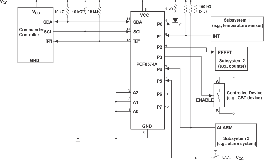
Typical Application

GUID-A5C6069C-D11D-4135-BC96-5B14361BD3A3-low.gif
The SCL and SDA pins must be pulled up to VCC because if SCL and SDA are pulled up to an auxiliary power supply that could be powered on while VCC is powered off, then the supply current, ICC, will increase as a result.
Device address is configured as 0111000 for this example.
P0, P2, and P3 are configured as outputs.
P1, P4, and P5 are configured as inputs.
P6 and P7 are not used and must be configured as outputs.
Figure 9-1 Application Schematic