ZHCSFL9 October   2016 OPT3006

PRODUCTION DATA.  

  1. 特性
  2. 应用
  3. 说明
  4. 修订历史记录
  5. Pin Configuration and Functions
  6. Specifications
    1. 6.1 Absolute Maximum Ratings
    2. 6.2 ESD Ratings
    3. 6.3 Recommended Operating Conditions
    4. 6.4 Thermal Information
    5. 6.5 Electrical Characteristics
    6. 6.6 Timing Requirements
    7. 6.7 Typical Characteristics
  7. Detailed Description
    1. 7.1 Overview
    2. 7.2 Functional Block Diagram
    3. 7.3 Feature Description
      1. 7.3.1 Human Eye Matching
      2. 7.3.2 Automatic Full-Scale Range Setting
      3. 7.3.3 Interrupt Operation, INT Pin, and Interrupt Reporting Mechanisms
      4. 7.3.4 I2C Bus Overview
        1. 7.3.4.1 Serial Bus Address
        2. 7.3.4.2 Serial Interface
    4. 7.4 Device Functional Modes
      1. 7.4.1 Automatic Full-Scale Setting Mode
      2. 7.4.2 Interrupt Reporting Mechanism Modes
        1. 7.4.2.1 Latched Window-Style Comparison Mode
        2. 7.4.2.2 Transparent Hysteresis-Style Comparison Mode
        3. 7.4.2.3 End-of-Conversion Mode
        4. 7.4.2.4 End-of-Conversion and Transparent Hysteresis-Style Comparison Mode
    5. 7.5 Programming
      1. 7.5.1 Writing and Reading
        1. 7.5.1.1 High-Speed I2C Mode
        2. 7.5.1.2 General-Call Reset Command
        3. 7.5.1.3 SMBus Alert Response
    6. 7.6 Register Maps
      1. 7.6.1 Internal Registers
        1. 7.6.1.1 Register Descriptions
          1. 7.6.1.1.1 Result Register (offset = 00h)
          2. 7.6.1.1.2 Configuration Register (offset = 01h) [reset = C810h]
          3. 7.6.1.1.3 Low-Limit Register (offset = 02h) [reset = C0000h]
          4. 7.6.1.1.4 High-Limit Register (offset = 03h) [reset = BFFFh]
          5. 7.6.1.1.5 Manufacturer ID Register (offset = 7Eh) [reset = 5449h]
          6. 7.6.1.1.6 Device ID Register (offset = 7Fh) [reset = 3001h]
  8. Application and Implementation
    1. 8.1 Application Information
      1. 8.1.1 Electrical Interface
      2. 8.1.2 Optical Interface
    2. 8.2 Typical Application
      1. 8.2.1 Design Requirements
      2. 8.2.2 Detailed Design Procedure
        1. 8.2.2.1 Optomechanical Design
      3. 8.2.3 Application Curves
    3. 8.3 Do's and Don'ts
  9. Power-Supply Recommendations
  10. 10Layout
    1. 10.1 Layout Guidelines
    2. 10.2 Soldering and Handling Recommendations
      1. 10.2.1 Solder Paste
      2. 10.2.2 Package Placement
      3. 10.2.3 Reflow Profile
      4. 10.2.4 Special Flexible Printed Circuit Board (FPCB) Recommendations
      5. 10.2.5 Rework Process
    3. 10.3 Layout Example
  11. 11器件和文档支持
    1. 11.1 文档支持
      1. 11.1.1 相关文档 
    2. 11.2 接收文档更新通知
    3. 11.3 社区资源
    4. 11.4 商标
    5. 11.5 静电放电警告
    6. 11.6 Glossary
  12. 12机械、封装和可订购信息

封装选项

机械数据 (封装 | 引脚)
散热焊盘机械数据 (封装 | 引脚)
订购信息

Pin Configuration and Functions

YMF Package
6-Pin PicoStar
Top View
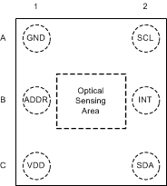
OPT3006 aij_OPT3006_Pinout.gif

Pin Functions

PIN I/O DESCRIPTION
NO. NAME
A1 GND Power Ground
B1 ADDR Digital input Address pin. This pin sets the LSBs of the I2C address.
C1 VDD Power Device power. Connect to a 1.6-V to 3.6-V supply.
A2 SCL Digital input I2C clock. Connect with a 10-kΩ resistor to a 1.6-V to 5.5-V supply.
B2 INT Digital output Interrupt output open-drain. Connect with a 10-kΩ resistor to a 1.6-V to 5.5-V supply.
C2 SDA Digital input/output I2C data. Connect with a 10-kΩ resistor to a 1.6-V to 5.5-V supply.