ZHCSK40D August 2019 – July 2020 OPA810
PRODUCTION DATA
- 1 特性
- 2 应用
- 3 说明
- 4 Revision History
- 5 Device Comparison Table
- 6 Pin Configuration and Functions
-
7 Specifications
- 7.1 Absolute Maximum Ratings
- 7.2 ESD Ratings
- 7.3 Recommended Operating Conditions
- 7.4 Thermal Information
- 7.5 Electrical Characteristics: 10 V
- 7.6 Electrical Characteristics: 24 V
- 7.7 Electrical Characteristics: 5 V
- 7.8 Typical Characteristics: VS = 10 V
- 7.9 Typical Characteristics: VS = 24 V
- 7.10 Typical Characteristics: VS = 5 V
- 7.11 Typical Characteristics: ±2.375-V to ±12-V Split Supply
- 8 Detailed Description
- 9 Application and Implementation
- 10Power Supply Recommendations
- 11Layout
- 12Device and Documentation Support
封装选项
机械数据 (封装 | 引脚)
散热焊盘机械数据 (封装 | 引脚)
订购信息
9.2.2 High-Z Input Data Acquisition Front-End
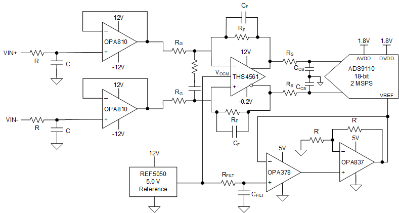
An ideal data acquisition system must measure a parameter without altering the measurand. When measuring a voltage or current from sensors with a large output impedance, an extremely high input impedance front-end with a pA range bias current is needed. Figure 9-15 shows an example circuit with the OPA810 used at the front-end. For systems with large input voltage attenuated with the MΩ range resistor divider, the OPA810 with its pA range bias currents adds negligible offset voltage and distortion because of the bias current induced resistor voltage drops. This circuit shows a funneling architecture with the OPA810 FET-input amplifier used as a unity-gain buffer, followed by attenuation to the ADS9110 5-V, full-scale input range and the ADC input drive using the THS4561 fully-differential amplifier (FDA). The THS4561 helps achieve better SNR and ENOB than a similar 5-V FDA, with a higher 12.6-V supply voltage and signal swings up to the ADC full-scale input range.
As a result of the capacitive switching and current inrush on the ADC VREF input pin, a wide bandwidth amplifier such as the OPA837 is used with the OPA378 in a composite loop as a reference buffer. The OPA378, driven from the REF5050 5-V voltage reference, offers high precision and the OPA837 gives fast-settling performance for the ADC reference input drive. See the Reference Design Maximizing Signal Dynamic Range for True 10 Vpp Differential Input to 20 bit ADC design guide for more a detailed analysis of this high-Z front-end.
 Figure 9-15 High-Z Input Data Acquisition Front-End