SBOS197F December 2001 – August 2015 OPA657
PRODUCTION DATA.
- 1 Features
- 2 Applications
- 3 Description
- 4 Revision History
- 5 Related Operational Amplifier Products
- 6 Pin Configuration and Functions
- 7 Specifications
- 8 Detailed Description
- 9 Application and Implementation
- 10Power Supply Recommendations
- 11Layout
- 12Device and Documentation Support
- 13Mechanical, Packaging, and Orderable Information
7 Specifications
7.1 Absolute Maximum Ratings
over operating free-air temperature range (unless otherwise noted)(1)| MIN | MAX | UNIT | ||
|---|---|---|---|---|
| Supply voltage (Total Bipolar Supplies) | ±6.5 | V | ||
| Internal power dissipation | See Thermal Information | |||
| Differential input voltage | –VS | +VS | V | |
| Input voltage | –VS | +VS | V | |
| Junction temperature (TJ) | 175 | °C | ||
| Storage temperature | –65 | 125 | °C | |
(1) Stresses beyond those listed under Absolute Maximum Ratings may cause permanent damage to the device. These are stress ratings only, which do not imply functional operation of the device at these or any other conditions beyond those indicated under Recommended Operating Conditions. Exposure to absolute-maximum-rated conditions for extended periods may affect device reliability.
7.2 ESD Ratings
| VALUE | UNIT | |||
|---|---|---|---|---|
| V(ESD) | Electrostatic discharge | Human-body model (HBM), per ANSI/ESDA/JEDEC JS-001(1) | ±2000 | V |
| Charged-device model (CDM), per JEDEC specification JESD22-C101(2) | ±500 | |||
| Machine Model (MM) | ±200 | |||
(1) JEDEC document JEP155 states that 500-V HBM allows safe manufacturing with a standard ESD control process.
(2) JEDEC document JEP157 states that 250-V CDM allows safe manufacturing with a standard ESD control process.
7.3 Recommended Operating Conditions
over operating free-air temperature range (unless otherwise noted)| MIN | NOM | MAX | UNIT | ||
|---|---|---|---|---|---|
| VS | Total supply voltage | 8 | 10 | 12 | V |
| TA | Ambient temperature | –40 | 25 | 85 | °C |
7.4 Thermal Information
| THERMAL METRIC(1) | OPA657 | UNIT | ||
|---|---|---|---|---|
| D (SOIC) | DBV (SOT-23) | |||
| 8 PINS | 5 PINS | |||
| RθJA | Junction-to-ambient thermal resistance | 125 | 150 | °C/W |
| RθJC(top) | Junction-to-case (top) thermal resistance | 85.2 | 140.8 | °C/W |
| RθJB | Junction-to-board thermal resistance | 75.9 | 62.8 | °C/W |
| ψJT | Junction-to-top characterization parameter | 26.2 | 24.4 | °C/W |
| ψJB | Junction-to-board characterization parameter | 75.4 | 61.8 | °C/W |
| RθJC(bot) | Junction-to-case (bottom) thermal resistance | — | — | °C/W |
(1) For more information about traditional and new thermal metrics, see the Semiconductor and IC Package Thermal Metrics application report, SPRA953.
7.5 Electrical Characteristics: VS = ±5 V
At RF = +453 Ω, RL = +100 Ω, and G = +10 V/V, unless otherwise noted. See Figure 29 for AC performance.| PARAMETER | TEST CONDITIONS | MIN | TYP | MAX | UNIT | TEST LEVEL(1) | ||
|---|---|---|---|---|---|---|---|---|
| AC PERFORMANCE (see Figure 29) | ||||||||
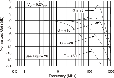
| Small-signal bandwidth | G = +7 V/V, VO = 200 mVPP | TJ = 25°C | 350 | MHz | C | |||
| G = +10 V/V, VO = 200 mVPP | TJ = 25°C | 275 | ||||||
| G = +20 V/V, VO = 200 mVPP | TJ = 25°C | 90 | ||||||
| Gain-bandwidth product | G > +40 V/V | TJ = 25°C | 1600 | dB | C | |||
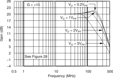
| Bandwidth for 0.1dB Flatness | G = +10 V/V, 2 VPP | TJ = 25°C | 30 | MHz | C | |||
| Peaking at a Gain of +7 | TJ = 25°C | 7 | dB | C | ||||
| Large-Signal Bandwidth | G = +10 V/V, 2 VPP | TJ = 25°C | 180 | MHz | C | |||
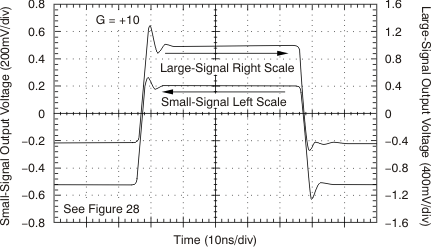
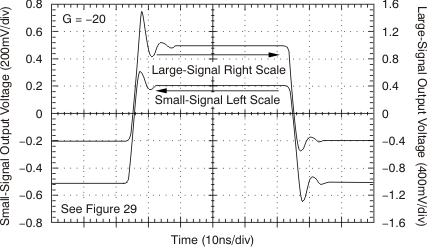
| Slew Rate | G = +10 V/V, 1-V Step | TJ = 25°C | 700 | V/μs | C | |||
| Rise-and-Fall Time | 0.2-V Step | TJ = 25°C | 1 | ns | C | |||
| Settling Time to 0.02% | G = +10 V/V, VO = 2-V Step | TJ = 25°C | 20 | ns | C | |||
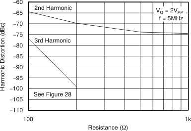
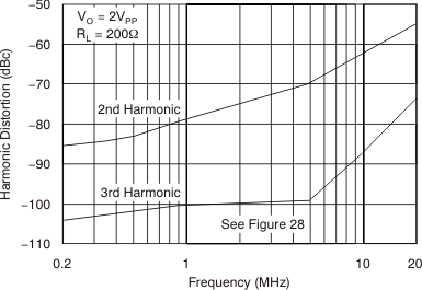
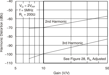
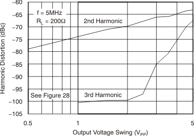
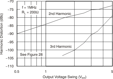
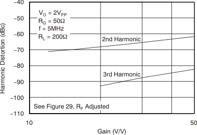
| Harmonic Distortion | G = +10 V/V, f = 5 MHz, VO = 2 VPP | C | ||||||
| 2nd-Harmonic | RL = 200 Ω | TJ = 25°C | –70 | dBc | C | |||
| RL > 500 Ω | TJ = 25°C | –74 | dBc | C | ||||
| 3rd-Harmonic | RL = 200 Ω | TJ = 25°C | –99 | dBc | C | |||
| RL > 500 Ω | TJ = 25°C | –106 | dBc | C | ||||
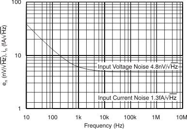
| Input Voltage Noise | f > 100 kHz | TJ = 25°C | 4.8 | nV/√Hz | C | |||
| Input Current Noise | f > 100 kHz | TJ = 25°C | 1.3 | fA/√Hz | C | |||
| DC PERFORMANCE(2) | ||||||||
| Open-Loop Voltage Gain (AOL) | VCM = 0 V, RL = 100 Ω | TJ = 25°C | 65 | 70 | dB | A | ||
| TJ = 0°C to 70°C(3) | 64 | |||||||
| TJ = –40°C to 85°C(3) | 63 | |||||||
| Input Offset Voltage | VCM = 0 V | TJ = 25°C | ±0.25 | ±1.8 | mV | A | ||
| TJ = 0°C to 70°C(3) | ±2.2 | |||||||
| TJ = –40°C to 85°C(3) | ±2.6 | |||||||
| Average Offset Voltage Drift | VCM = 0 V | TJ = 25°C | ±12 | ±2 | μV/°C | A | ||
| TJ = 0°C to 70°C(3) | ±12 | |||||||
| TJ = –40°C to 85°C(3) | ±12 | |||||||
| Input Bias Current | VCM = 0 V | TJ = 25°C | ±2 | ±20 | pA | A | ||
| TJ = 0°C to 70°C(3) | ±1800 | |||||||
| TJ = –40°C to 85°C(3) | ±5000 | |||||||
| Input Offset Current | VCM = 0 V | TJ = 25°C | ±1 | ±10 | pA | A | ||
| TJ = 0°C to 70°C(3) | ±900 | |||||||
| TJ = –40°C to 85°C(3) | ±2500 | |||||||
| INPUT | ||||||||
| Most Positive Input Voltage(3) | TJ = 25°C | 2 | 2.5 | V | A | |||
| TJ = 0°C to 70°C(3) | 1.9 | |||||||
| TJ = –40°C to 85°C(3) | 1.8 | |||||||
| Most Negative Input Voltage(3) | TJ = 25°C | –3.5 | –4 | V | A | |||
| TJ = 0°C to 70°C(3) | –3.4 | |||||||
| TJ = –40°C to 85°C(3) | –3.3 | |||||||
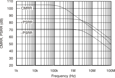
| Common-Mode Rejection Ratio (CMRR) | VCM = ±0.5 V | TJ = 25°C | 83 | 89 | dB | A | ||
| TJ = 0°C to 70°C(3) | 81 | |||||||
| TJ = –40°C to 85°C(3) | 79 | |||||||
| Input Impendance | ||||||||
| Differential | TJ = 25°C | 1012 || 0.7 | Ω || pF | C | ||||
| Common-Mode | TJ = 25°C | 1012 || 4.5 | Ω || pF | C | ||||
| OUTPUT | ||||||||
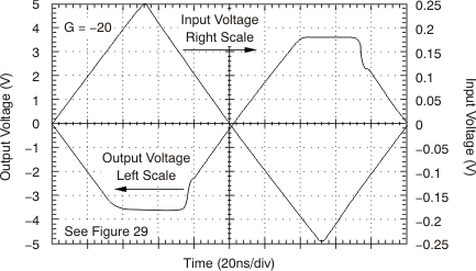
| Voltage Output Swing | No load | TJ = 25°C | ±3.9 | V | A | |||
| TJ = 0°C to 70°C(3) | ±3.7 | |||||||
| RL = 100 Ω | TJ = 25°C | ±3.3 | ±3.5 | V | B | |||
| TJ = 0°C to 70°C(3) | ±3.2 | |||||||
| TJ = –40°C to 85°C(3) | ±3.1 | |||||||
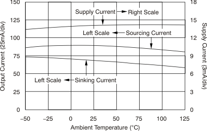
| Current Output, Sourcing | TJ = 25°C | 50 | 70 | mA | A | |||
| TJ = 0°C to 70°C(3) | 48 | |||||||
| TJ = –40°C to 85°C(3) | 46 | |||||||
| Current Output, Sinking | TJ = 25°C | –50 | –70 | mA | A | |||
| TJ = 0°C to 70°C(3) | –48 | |||||||
| TJ = –40°C to 85°C(3) | –46 | |||||||
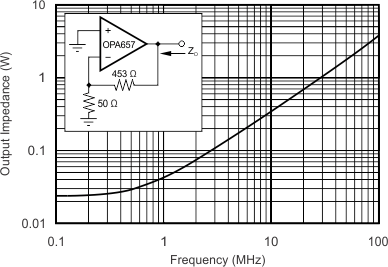
| Closed-Loop Output Impedance | G = +10 V/V, f = 0.1 MHz | TJ = 25°C | 0.02 | Ω | A | |||
| POWER SUPPLY | ||||||||
| Specified Operating Voltage | TJ = 25°C | ±5 | V | A | ||||
| Minimum Operating Voltage | TJ = 25°C | ±4 | V | C | ||||
| Maximum Operating Voltage Range | TJ = 25°C | ±6 | V | A | ||||
| TJ = 0°C to 70°C(3) | ±6 | |||||||
| TJ = –40°C to 85°C(3) | ±6 | |||||||
| Maximum Quiescent Current | TJ = 25°C | 14 | 16 | mA | A | |||
| TJ = 0°C to 70°C(3) | 16.2 | |||||||
| TJ = –40°C to 85°C(3) | 16.3 | |||||||
| Minimum Quiescent Current | TJ = 25°C | 11.7 | 14 | mA | A | |||
| TJ = 0°C to 70°C(3) | 11.4 | |||||||
| TJ = –40°C to 85°C(3) | 11.1 | |||||||
| Power-Supply Rejection Ratio (+PSRR) | +VS = 4.5 V to 5.5 V | TJ = 25°C | 76 | 80 | dB | A | ||
| TJ = 0°C to 70°C(3) | 74 | |||||||
| TJ = –40°C to 85°C(3) | 72 | |||||||
| Power-Supply Rejection Ratio (–PSRR) | –VS = 4.5 V to 5.5 V | TJ = 25°C | 62 | 68 | dB | A | ||
| TJ = 0°C to 70°C(3) | 60 | |||||||
| TJ = –40°C to 85°C(3) | 58 | |||||||
| TEMPERATURE RANGE | ||||||||
| Specified Operating Range: U, N Package | TJ = 25°C | –40 to +85 | °C | |||||
| Thermal Resistance, RθJA | Junction-to-Ambient | |||||||
| U: SO-8 | TJ = 25°C | 125 | °C/W | |||||
| N: SOT23-5 | TJ = 25°C | 150 | °C/W | |||||
(1) Test Levels: (A) 100% tested at +25°C. Over-temperature limits by characterization and simulation. (B) Limits set by characterization and simulation. (C) Typical value only for information.
(2) Current is considered positive out-of-node. VCM is the input common-mode voltage.
(3) Tested < 3dB below minimum specified CMRR at ±CMIR limits.
7.6 Electrical Characteristics: VS - ±5 V, High-Grade DC Specifications
At RF = 453 Ω, RL = 100 Ω, and G = +10 V/V, unless otherwise noted. (1)| PARAMETER | TEST CONDITIONS | MIN | TYP | MAX | UNIT | TEST LEVEL(4) | ||
|---|---|---|---|---|---|---|---|---|
| Input Offset Voltage | VCM = 0 V | TJ = 25°C | ±0.1 | ±0.6(2) | mV | A | ||
| TJ = 0°C to 70°C(3) | ±0.85 | |||||||
| TJ = –40°C to 85°C(3) | ±0.9 | |||||||
| Input Offset Voltage Drift | VCM = 0 V | TJ = 25°C | ±2 | ±6(2) | μV/°C | A | ||
| TJ = 0°C to 70°C(3) | ±6 | |||||||
| TJ = –40°C to 85°C(3) | ±6 | |||||||
| Input Bias Current | VCM = 0 V | TJ = 25°C | ±1 | ±5(2) | pA | A | ||
| TJ = 0°C to 70°C(3) | ±450 | |||||||
| TJ = –40°C to 85°C(3) | ±1250 | |||||||
| Input Offset Current | VCM = 0 V | TJ = 25°C | ±0.5 | ±5(2) | pA | A | ||
| TJ = 0°C to 70°C(3) | ±450 | |||||||
| TJ = –40°C to 85°C(3) | ±1250 | |||||||
| Common-Mode Rejection Ratio (CMRR) | VCM = ±0.5 V | TJ = 25°C | 91(2) | 98 | dB | A | ||
| TJ = 0°C to 70°C(3) | 89 | |||||||
| TJ = –40°C to 85°C(3) | 87 | |||||||
| Power-Supply Rejection Ratio (+PSRR) | +VS = 4.5 V to 5.5 V | TJ = 25°C | 78(2) | 82 | dB | A | ||
| TJ = 0°C to 70°C(3) | 76 | |||||||
| TJ = –40°C to 85°C(3) | 74 | |||||||
| Power-Supply Rejection Ratio (–PSRR) | –VS = –4.5 V to –5.5 V | TJ = 25°C | 68(2) | 74 | dB | A | ||
| TJ = 0°C to 70°C(3) | 66 | |||||||
| TJ = –40°C to 85°C(3) | 64 | |||||||
(1) All other specifications are the same as the standard-grade.
(2) Junction temperature = ambient for +25°C specifications.
(3) Junction temperature = ambient at low temperature limit: junction temperature = ambient +20°C at high temperature limit for over temperature specifications.
(4) Test Levels: (A) 100% tested at +25°C. Over temperature limits by characterization and simulation.
7.7 Typical Characteristics: VS = ±5 V
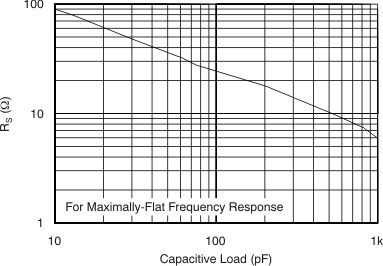
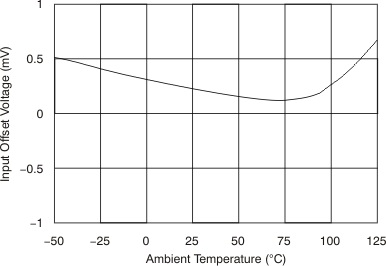
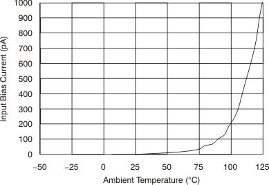
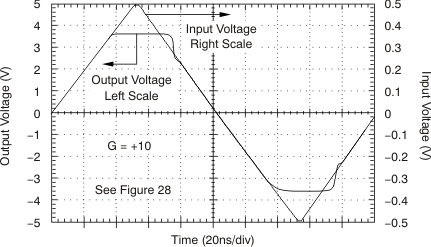
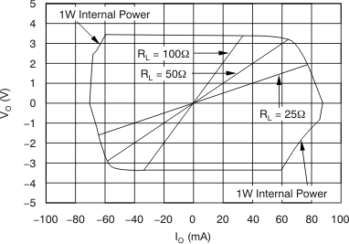
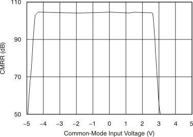
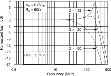
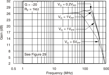
At TA = 25°C, G = 10 V/V, RF = 453 Ω, and RL = 100 Ω, unless otherwise noted.