ZHCSDL0A April   2015  – October 2015 OPA2625 , OPA625

PRODUCTION DATA.  

  1. 特性
  2. 应用
  3. 说明
  4. 修订历史记录
  5. Pin Configuration and Functions
  6. Specifications
    1. 6.1  Absolute Maximum Ratings
    2. 6.2  ESD Ratings
    3. 6.3  Recommended Operating Conditions
    4. 6.4  Thermal Information
    5. 6.5  Electrical Characteristics High-Drive Mode
    6. 6.6  Electrical Characteristics Low-Power Mode
    7. 6.7  Electrical Characteristics High-Drive Mode
    8. 6.8  Electrical Characteristics Low-Power Mode
    9. 6.9  Switching Characteristics
    10. 6.10 Typical Characteristics
  7. Parameter Measurement Information
    1. 7.1 DC Parameter Measurements
    2. 7.2 Transient Parameter Measurements
    3. 7.3 AC Parameter Measurements
    4. 7.4 Noise Parameter Measurements
  8. Detailed Description
    1. 8.1 Overview
    2. 8.2 Functional Block Diagram
    3. 8.3 Feature Description
      1. 8.3.1 SAR ADC Driver
      2. 8.3.2 Electrical Overstress
    4. 8.4 Device Functional Modes
      1. 8.4.1 High-Drive Mode
      2. 8.4.2 Low-Power Mode
  9. Application and Implementation
    1. 9.1 Application Information
    2. 9.2 Typical Applications
      1. 9.2.1 Single-Supply, 16-Bit, 1-MSPS SAR ADC Driver
        1. 9.2.1.1 Design Requirements
        2. 9.2.1.2 Detailed Design Procedure
        3. 9.2.1.3 Application Curves
      2. 9.2.2 Single-Supply, 16-Bit, 1-MSPS, Multiplexed, SAR ADC Driver
        1. 9.2.2.1 Design Requirements
        2. 9.2.2.2 Detailed Design Procedure
        3. 9.2.2.3 Application Curves
  10. 10Power Supply Recommendations
  11. 11Layout
    1. 11.1 Layout Guidelines
    2. 11.2 Layout Example
  12. 12器件和文档支持
    1. 12.1 器件支持
      1. 12.1.1 开发支持
        1. 12.1.1.1 TINA-TI(免费软件下载)
        2. 12.1.1.2 TI 高精度设计
    2. 12.2 文档支持
      1. 12.2.1 相关文档
    3. 12.3 相关链接
    4. 12.4 Community Resources
    5. 12.5 商标
    6. 12.6 静电放电警告
    7. 12.7 Glossary
  13. 13机械、封装和可订购信息

封装选项

机械数据 (封装 | 引脚)
散热焊盘机械数据 (封装 | 引脚)
订购信息

5 Pin Configuration and Functions

OPA625: DBV Package
6-Pin SOT
Top View
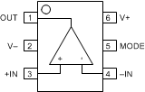
OPA625 OPA2625 6-PIN_DBV.gif
OPA2625: DGS Package
10-Pin VSSOP
Top View
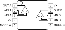
OPA625 OPA2625 10_PIN_DGS_SBOS688.gif

Pin Functions: OPA625

PIN I/O DESCRIPTION
NAME NO
+IN 3 I Noninverting input
–IN 4 I Inverting input
MODE 5 I Controls OPA625 mode:
V+ = low-power mode
V– = high-drive mode
NOTE: Do not float this pin.
OUT 1 O Output terminal
V+ 6 Positive supply voltage
V– 2 Negative supply voltage

Pin Functions: OPA2625

PIN I/O DESCRIPTION
NAME NO.
+IN A 3 I Noninverting input for channel A
–IN A 2 I Inverting input for channel A
+IN B 7 I Noninverting input for channel B
–IN B 8 I Inverting input for channel B
MODE A 5 I Controls OPA2625 mode for channel A:
V+ = low-power mode
V– = high-drive mode
NOTE: Do not float this pin.
MODE B 6 I Controls OPA2625 mode for channel B:
V+ = low-power mode
V– = high-drive mode
NOTE: Do not float this pin.
OUT A 1 O Output terminal for channel A
OUT B 9 O Output terminal for channel B
V+ 10 Positive supply voltage
V– 4 Negative supply voltage