ZHCSI30G March 2002 – April 2018 OPA2354 , OPA354 , OPA4354
PRODUCTION DATA.
- 1 特性
- 2 应用
- 3 说明
- 4 修订历史记录
- 5 Device Comparison Table
- 6 Pin Configuration and Functions
- 7 Specifications
- 8 Detailed Description
- 9 Application and Implementation
- 10Power Supply Recommendations
- 11Layout
- 12器件和文档支持
- 13机械、封装和可订购信息
封装选项
机械数据 (封装 | 引脚)
散热焊盘机械数据 (封装 | 引脚)
- DDA|8
订购信息
6 Pin Configuration and Functions
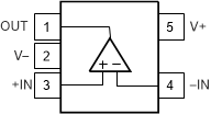
OPA354 DBV Package
5-Pin SOT-23
Top View

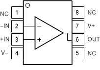
8-Pin HSOP
Top View

NC – no internal connection
PowerPAD must be connected to V− or left floating.
Pin Functions: OPA354
| PIN | I/O | DESCRIPTION | ||
|---|---|---|---|---|
| NAME | SOT-23 | HSOP | ||
| –IN | 4 | 2 | I | Inverting input |
| +IN | 3 | 3 | I | Noninverting input |
| NC | — | 1, 5, 8 | — | No internal connection (can be left floating) |
| OUT | 1 | 6 | O | Output |
| V– | 2 | 4 | — | Negative (lowest) supply |
| V+ | 5 | 7 | — | Positive (highest) supply |
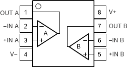
OPA2354 DGK and DDA Packages1
8-Pin VSSOP, HSOP
Top View

1. PowerPAD must be connected to V− or left floating.
Pin Functions: OPA2354
| PIN | I/O | DESCRIPTION | |
|---|---|---|---|
| NAME | NO. | ||
| –IN A | 2 | I | Inverting input, channel A |
| +IN A | 3 | I | Noninverting input, channel A |
| –IN B | 6 | I | Inverting input, channel B |
| +IN B | 5 | I | Noninverting input, channel B |
| OUT A | 1 | O | Output, channel A |
| OUT B | 7 | O | Output, channel B |
| V– | 4 | — | Negative (lowest) supply |
| V+ | 8 | — | Positive (highest) supply |
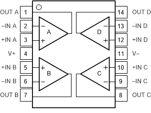
OPA4354 D and PW Packages
14-Pin SOIC, TSSOP
Top View

Pin Functions: OPA4354
| PIN | I/O | DESCRIPTION | |
|---|---|---|---|
| NAME | NO. | ||
| –IN A | 2 | I | Inverting input, channel A |
| +IN A | 3 | I | Noninverting input, channel A |
| –IN B | 6 | I | Inverting input, channel B |
| +IN B | 5 | I | Noninverting input, channel B |
| –IN C | 9 | I | Inverting input, channel C |
| +IN C | 10 | I | Noninverting input, channel C |
| –IN D | 13 | I | Inverting input, channel D |
| +IN D | 12 | I | Noninverting input, channel D |
| OUT A | 1 | O | Output, channel A |
| OUT B | 7 | O | Output, channel B |
| OUT C | 8 | O | Output, channel C |
| OUT D | 14 | O | Output, channel D |
| V– | 11 | — | Negative (lowest) supply |
| V+ | 4 | — | Positive (highest) supply |